Circuit boards in operation contain many heat-generating components such as MOSFETs, LEDs, and transistors, especially under full-load conditions. Thermal vias are a well-known method for dissipating heat from surface-mount components on PCBs.
Circuit boards in operation contain many heat-generating components such as MOSFETs, LEDs, and transistors, especially under full-load conditions. Thermal vias are a well-known method for dissipating heat from surface-mount components on PCBs. Structurally, vias are drilled and plated with copper to connect the top and bottom copper foils of single-sided or double-sided boards, increasing the area and volume available for heat dissipation and reducing thermal resistance. In multilayer boards, thermal vias can connect multiple layers or be limited to partial layer connections, but the fundamental principle remains the same.
Mounting the thermal pad of a surface-mount component on a PCB reduces thermal resistance. Thermal resistance depends on the area and thickness of the copper foil used for heat dissipation, as well as the thickness and material of the board. Essentially, wider and thicker materials provide better heat dissipation. However, copper foil thickness must comply with standard specifications and cannot be excessively thick. Additionally, since miniaturization remains a fundamental design requirement, PCB area should be designed according to actual needs, and copper foil thickness cannot be made very large. Therefore, when the single-sided heat dissipation area of a PCB exceeds a certain threshold, the heat dissipation effect of single-sided boards is significantly reduced. FR-4 has a very low thermal conductivity.
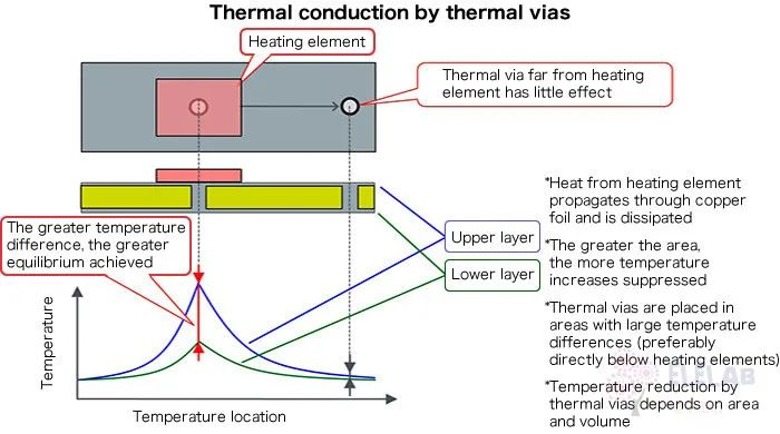
One measure to solve these problems is the use of thermal vias, which are formed by drilling and plating copper in the same way as PTH vias used for electrical interconnection between layers. To use thermal vias effectively, they should be placed close to the heating element. As shown in the figure below, this leverages the effect of thermal equilibrium, making it clear that connecting areas with large temperature differences provides excellent results.
Effect of Hollow vs. Filled Vias
Hollow vias result in higher thermal resistance compared to filled vias. For a 0.6mm diameter via with 35μm (1 oz.) copper plating, the area perpendicular to the thermal pad is only 0.06 mm², resulting in a thermal resistance of 64°C/W. In contrast, a solder-filled via has an area of 0.28 mm² and a thermal resistance of 42°C/W, while a fully copper-filled via has a thermal resistance of 14°C/W. Solid copper-filled vias further reduce thermal resistance compared to vias filled with SnAgCu solder.
Increasing the plating thickness during PCB manufacturing improves the thermal resistance of vias. In the example above, increasing the plating thickness to 70μm (2 oz.) reduces the thermal resistance per via to 34°C/W, but this increases PCB production costs.
In addition to creating solid vias during the plating process, another option is to fill vias with copper or other thermally conductive materials such as conductive epoxy during PCB manufacturing. However, this adds an extra step to the PCB manufacturing process and may increase board costs.
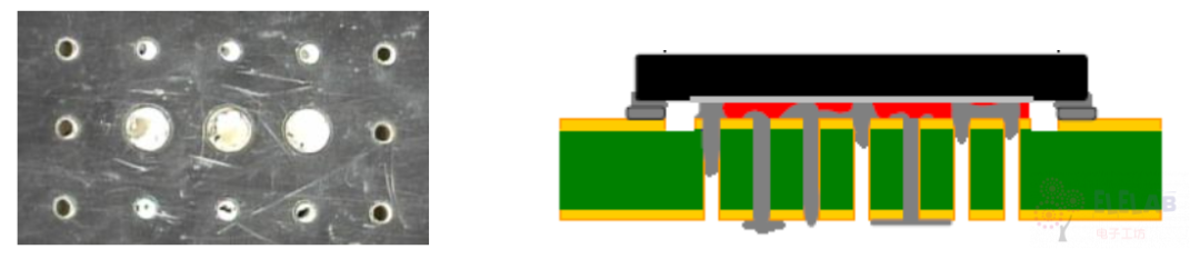
If large hollow vias are subjected to reflow soldering, unfilled vias may be filled with solder. However, this is affected by many factors, leading to solder wicking that reduces the effective pad connection area and causes reliability issues. If vias cannot be reliably grounded and filled, thermal conductivity will be compromised. The lower left figure below shows an example of an unfilled via after reflow, and the lower right figure shows an example of solder voids under the chip (indicated in red), which can be inspected by X-ray.
Voids increase the thermal resistance of the thermal interface. Similarly, excessive solder may cause bumps on the bottom of the board, reducing the contact area between the board and the heat sink.
Solder wicking can be limited by two methods:
- Keep via diameter below 0.3mm: For smaller vias, the surface tension of liquid solder inside the via better resists gravity. Constructing vias with an internal diameter of approximately 0.25mm-0.3mm minimizes solder wicking. The disadvantage of this method is that smaller openings result in higher overall thermal resistance.
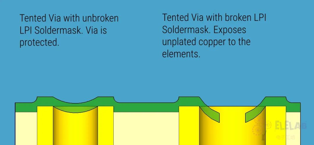
- Use solder mask for via tenting: This involves using solder mask to prevent solder from entering or exiting thermal vias, depending on which side of the board the solder mask is applied (some tenting may be imperfect). Top-side via tenting places a small area of solder mask over thermal vias on the top side of the PCB to prevent solder from flowing into the vias from the top side. The small via on the left in the figure below has an intact LPI solder mask that protects the via. The via on the right has a broken LPI solder mask due to the liquid nature of LPI solder mask and attempts to cover too large a span, resulting in solder leakage.
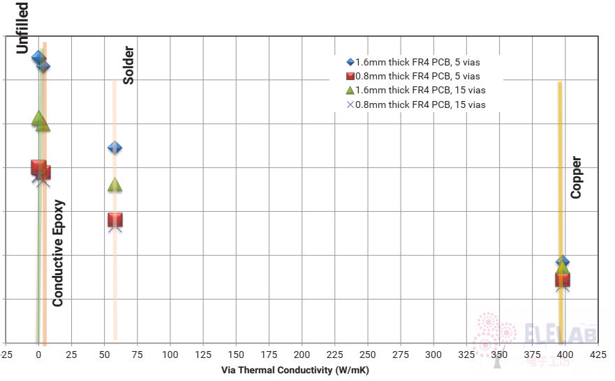
The thermal resistance analysis results for FR-4 vias filled with materials of different thermal conductivities show that solid copper-filled vias result in lower thermal resistance, while unfilled vias provide higher thermal resistance. Vias filled with conductive epoxy perform only slightly better than unfilled vias.
Effect of PCB Via Diameter and Number of Vias
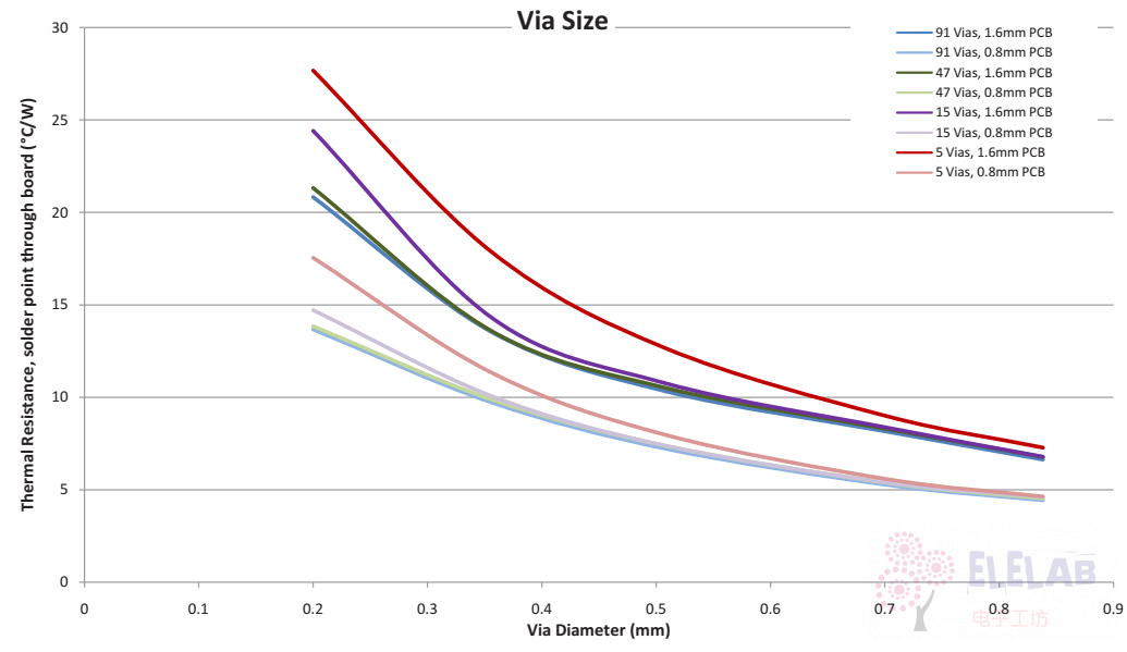
As explained in the previous section, larger solid vias have lower thermal resistance. However, instead of implementing expensive solid copper-plugged vias, increasing the number of vias also shows considerable improvement.
The simulation below shows the relationship between via diameter and thermal resistance.
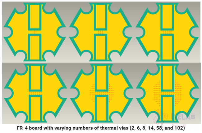
The next case considers the effect of changing the number of thermal vias. These vias are solid copper-plated, 10mil in diameter, with a center-to-center spacing of 25mil. This size was chosen because standard plating techniques can be used to fill the vias without additional processing. (14 vias is the maximum area for an LED device thermal pad).
The results shown in the figure below indicate that increasing the number of vias beyond 14 provides almost no improvement (this is the maximum achievable density perpendicular to the LED thermal pad).
Given that the total available area for thermal vias is usually fixed, using a large number of smaller vias to fill a larger portion of this area is recommended. A 0.3mm via is a reasonable size.
Effect of PCB Heat Dissipation Area
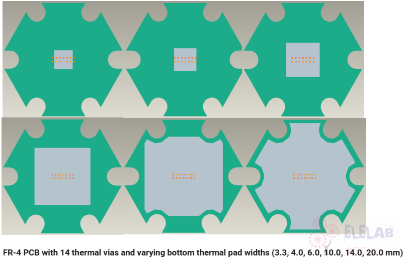
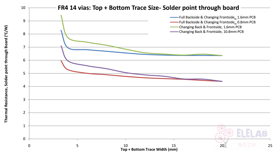
The figure below shows an FR-4 PCB with 14 copper-plated vias of 0.254mm diameter, with bottom thermal copper foil widths of 3.3, 4.0, 6.0, 10.0, 14.0, and 20.0mm.
The simulation results show that as the width of the bottom thermal pad increases, there is a small difference in thermal resistance. For 1.6mm thick boards, increasing the width beyond 12mm provides almost no improvement, while for 0.8mm thick boards, the improvement diminishes when the width exceeds 16mm.
Summary of Thermal Simulation Results
The simulation results show that to minimize the thermal resistance of FR-4 boards, the dielectric thickness should be reduced to 0.8mm.
While using a large number of vias reduces thermal resistance, the cost of manufacturing the board must also be considered. Larger unfilled vias increase the likelihood of partial via filling during soldering. Smaller solid-filled vias are a better solution.
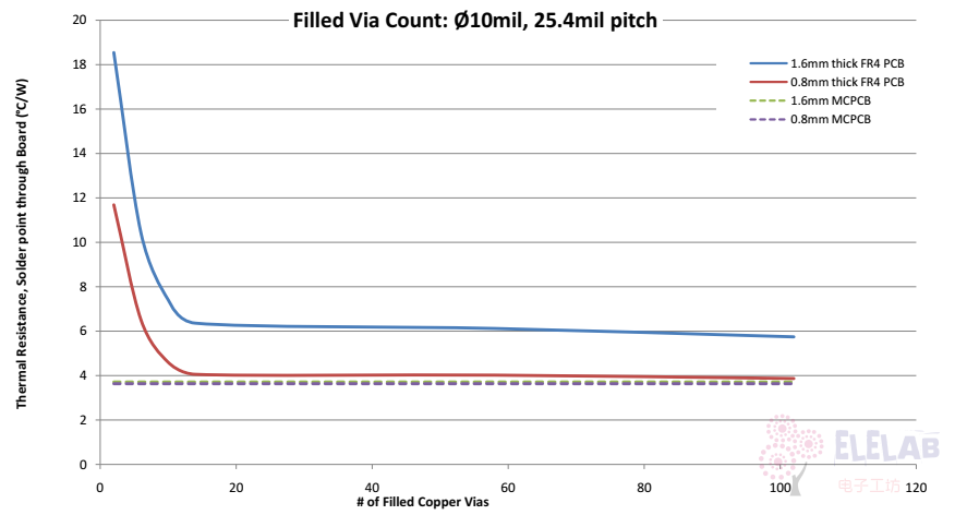
Finally, due to thermal diffusion resistance, the benefit of adding additional vias and increasing the width of the copper foil area decreases beyond a certain point. It is recommended to create a via area with 10mil (or 0.3mm for cost savings) vias. This parameter was chosen for its combination of performance and manufacturability. According to several PCB manufacturers, 10mil vias with 25mil spacing are a reasonable and repeatable production option when used with 2oz copper. Solid copper filling can be reliably achieved during the board plating process. The simulation in the final section on PCB via diameter and number of vias shows that 10mil vias can achieve a thermal resistance of 4°C/W (solid copper vias) on a 0.8mm FR-4 PCB.
 About Maxipcb
Maxipcb empowers innovators to turn cutting-edge technologies into reality.
We offer one-stop solutions for design, simulation, testing, PCB manufacturing, component procurement and SMT assembly, enabling efficient development, rapid deployment and risk control across the full product lifecycle.Serving the world in communications, industrial automation, aerospace, automotive, semiconductor and beyond, we build a safer, more connected future together.