
As important devices for radiating and receiving wireless signals, antennas play a key role in wireless communication. How exactly does an antenna realize the conversion of signals from wired to wireless? How can an antenna with excellent performance be designed? This series of articles takes you through an in-depth understanding.
What is a PCB antenna? As the name suggests, it is a trace printed on a PCB. It can be drawn as a straight trace, an inverted-F trace, a serpentine or circular trace, etc. A length of about one-quarter wavelength can basically form an antenna to radiate electrical signals outward or receive signals.
In the previous article (In-depth Interpretation of Antennas in Wireless Communication ① — Getting to Know Antennas), we introduced several key performance indicators of antennas: gain, operating frequency band/bandwidth, VSWR/input impedance. In this issue, referring to these key parameters, we take the ZM602 series Wi-Fi module launched by Guangzhou Zhiyuan Electronics Co., Ltd. as an example to see how to design a PCB antenna with excellent performance.
The table below shows the parameter specification requirements for this antenna design.
Table 1 Antenna Parameter Design Specifications
| Gain | >2.0dBi |
| Operating bandwidth | >150MHz |
| S11 within bandwidth | <-10dB |
| Input impedance | 50Ω |
| VSWR | <2.0 |
Antenna Model
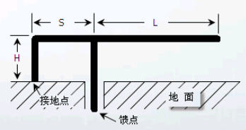
The most common structure of a PCB antenna is the inverted-F antenna, as shown in the figure below.

Figure 1 Inverted-F Antenna Model
The length of the antenna needs to match one-quarter of the free-space wavelength of the transmitted signal, so as to achieve the highest transmission and reception conversion efficiency and better produce a good input impedance. The free-space wavelength of a 2.45GHz signal is 122.45mm, so the corresponding antenna length is about 30.6mm. This length is the length of the inverted-F part (L) in the PCB antenna. In actual design, in order to reduce the space occupied by the antenna as much as possible, it is often designed as serpentine routing. The antenna height (H), the distance between the feed line and the ground point (S), and the width of the serpentine routing are parameters that need to be designed through specific simulation and debugging. Due to space limitations, they will not be expanded here.
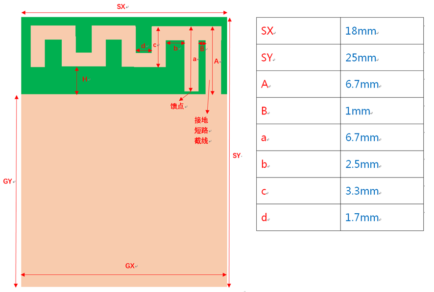
Figure 2 Serpentine Routing of the Antenna
In addition to the serpentine routing of the inverted-F part, the antenna also requires a good ground plane to achieve signal radiation and reception. The length requirement for the ground plane is the same as that of the serpentine routing part, namely one-quarter of the free-space wavelength of the transmitted signal, i.e., 30.6mm. Considering the actual usage environment of the product, the size of the wireless module cannot be too large. Therefore, in this design, we designed the overall size of the ZM602 module as 25*18mm, in which the maximum length of the ground plane is about 25mm (diagonal). Since the ground plane length cannot reach the 30.6mm requirement, the antenna performance is affected to some extent. However, if the ZM602 module is soldered onto a test baseboard or a customer baseboard, the ground plane of the baseboard can be used to allow the antenna to achieve the best performance.
After adjustment and optimization by simulation software, the final antenna model dimensions we determined are as follows.
Now, the PCB antenna of the ZM602 has been designed. Has the performance of this antenna met our design requirements? We simulated and tested the antenna in simulation software (with a test baseboard), and also conducted actual tests on the physical antenna. The test results show that all antenna parameters meet the design requirements.
About Maxipcb
Serving the world in communications, industrial automation, aerospace, automotive, semiconductor and beyond, we build a safer, more connected future together.