This application note discusses Maxim Integrated's BGA packages and provides PCB design and board assembly process guidelines.
This application note discusses Maxim Integrated's BGA packages and provides PCB design and board assembly process guidelines.
Introduction
Maxim's BGA packages consist of one or more dies connected to a laminate substrate using wire bonding or a flip-chip configuration. Some packages may contain surface-mount components (SMT), depending on the application. A representative cross-sectional image of the package is shown in Figure 1.
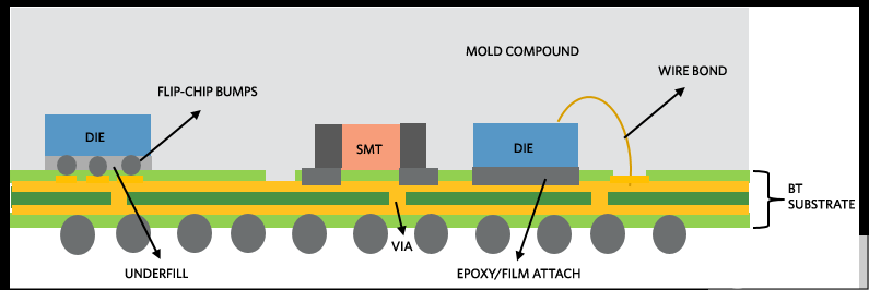
Figure 1. Cross-sectional view of a Maxim BGA package (not to scale).
PCB Design
Maxim BGA packages use solder-mask-defined (SMD) pins/balls.
Surface-mount devices use two types of pad patterns:
Solder-mask-defined (SMD) pads have a solder mask opening smaller than the metal pad.
Non-solder-mask-defined (NSMD) pads have a solder mask opening larger than the metal pad.
Maxim recommends using NSMD pads because of the following advantages: (i) the copper etching process has better control compared with solder mask, and (ii) NSMD provides a larger metal area for solder anchoring (pad area + vertical edge of the pad).
IPC-7351 guidelines can be used to design PCB land patterns based on the package outline drawing of the corresponding package. The IPC land pattern calculator is available for download from the IPC website (www.ipc.org).
For NSMD
The recommended PCB pad size is equal to the BGA ball size. The solder mask opening should be BGA ball size + 0.1 mm.
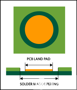
Figure 2. Illustration of an NSMD land pad pattern.
PCB Surface Finish
Selecting an appropriate PCB pad surface finish is critical to ensuring optimal manufacturing of the final board assembly. Common surface finishes for PCB pads are listed below:
OSP (organic solderability preservative)—recommended
ENIG (electroless nickel immersion gold)—recommended
Electroplated nickel, gold
Immersion silver
Immersion tin
Stencil Design
Stencil thickness and aperture geometry determine the precise volume of solder paste deposited onto the device land pattern. Stencil alignment accuracy and consistent solder volume transfer are critical for uniform solder reflow. Stainless steel stencils are preferred. The stencil should be laser-cut and then electropolished for better paste release than conventional laser-cut stencils.
The recommended stencil thickness is 4 mil (0.100 mm).
Stencil apertures are recommended to be circular and the same size as the PCB pad. Tolerances must be tightly controlled because they can effectively reduce aperture size. Aperture walls should be: (i) smooth, and (ii) have a trapezoidal cross-section (bottom opening larger than top) to enhance solder paste release from the aperture. The stencil aperture must meet the industry-standard area ratio (aperture opening area / aperture wall area) > 0.66.
Solder Paste
A low-residue, no-clean solder paste is recommended for mounting BGA packages. Type III or Type IV solder paste is best suited for the typical pitches in Maxim modules. Nitrogen purge during solder reflow is recommended. Follow the paste supplier's recommended stencil cleaning frequency for the corresponding solder paste.
Recommended solder paste compositions are shown below:
Lead-free (recommended): SAC (tin-silver-copper) alloy (SAC305)
Lead-based: tin/lead alloy (Sn63Pb37)
Screen Printing
A metal squeegee with a 45° to 60° print angle should be used. For printing, 20 mm/sec should be used as the starting speed, increasing speed as needed. A pressure of ~10 N/mm should be applied during squeegee printing. The snap-off distance should be 0 mm. In addition, post-print solder inspection is recommended to check print quality.
Placement
A standard pick-and-place machine with 0.05 mm accuracy can be used to place the BGA module onto the printed solder paste. A lower placement speed is recommended to prevent paste squeeze-out.
Reflow
A forced convection oven with nitrogen and temperature uniformity within ±5°C is recommended. The reflow profile guidelines in the solder paste datasheet should be followed. This guideline is based on the temperature at the actual joint location; the actual solder joint temperature usually differs from the temperature settings in the reflow system depending on board density, board thickness, and other components mounted on the board. It is recommended to use a thermocouple at the solder joint location to check the profile before reflow for actual board interconnection. Figure 3 shows the recommended reflow profile for lead-free solder, compliant with JEDEC JSTD-020.
Double-sided reflow should not be performed on these BGA modules.
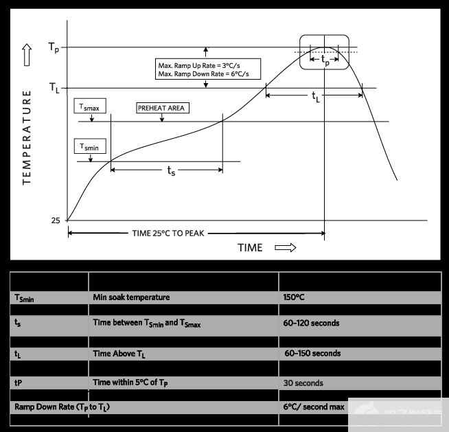
Figure 3. Recommended lead-free solder reflow profile compliant with JEDEC JSTD-020.
Cleaning
If a low-residue, no-clean solder paste is used, cleaning is usually not required. It is recommended to follow the supplier's cleaning guidelines. If cleaning is performed, the board needs to be dried afterward.
Solder Joint Voids
IPC recommends a maximum void specification of 25% for solder joints. If a higher void percentage is observed, increasing the soak time can be evaluated as an option.
Rework
Component Removal
An appropriate rework station should be used for any rework of the part. It is strongly recommended to bake the assembled PCB at 125°C for 24 hours to eliminate residual moisture before removing the component. The bottom of the PCB should be heated with a convection heater while the top of the component is heated with hot air or gas (this is to prevent warping). A special nozzle should be used to direct air to the component so as to reduce heating of adjacent components. Thermocouples should be used on the top and bottom to monitor the actual temperature of the part. The maximum part temperature should be above the liquidus temperature of 217°C but should not exceed 260°C. After joint reflow, vacuum lift-off should automatically engage during the transition from reflow to cooling. Vacuum pressure should be maintained below 15 inches of mercury to ensure that the component is not lifted out if all joints have not reflowed.
Site Remediation
After removing the component, the PCB site should be properly cleaned, while taking care that the pads are not damaged. Then apply solvent to clean the PCB pads; the solvent is usually specific to the type of paste used in the original assembly. The paste manufacturer's recommendations should be followed.
Solder Paste Printing
It is recommended to use a micro stencil to print solder paste on the PCB surface at the component site. Follow the stencil thickness, stencil design, soldering recommendations, and screen printing guidelines as in the original PCB assembly. Inspect the site before replacing the new component.
Component Placement
A new replacement component should be used; use of the removed part is not recommended. Beam-splitter optics should be used to align the component on the PCB (because the leads are on the bottom of the package), as this will provide an overlay image of the leads on the mating package and help with correct alignment. A pick-and-place machine with 0.05 mm placement accuracy should be used.
Reflow
It is recommended to use the same reflow profile as the initial component attachment reflow. X-ray can be used to ensure that all joints are successfully formed.
Unit Shipping
Parts will be shipped in trays or tape and reel. All parts will be baked and dry-packed with desiccant and a humidity indicator card. If the humidity indicator card turns pink, or if the parts have been exposed beyond their floor life after packaging, they should be baked at 125°C for 48 hours. Refer to JEDEC specification J-STD-033C for proper handling of moisture/reflow-sensitive surface-mount devices.
Maximum Allowable Downward Pressure That Can Be Applied to Maxim BGA Packages
The following guidelines should be followed to determine the maximum downward pressure that can be applied to the top of Maxim BGA packages. These guidelines assume that the printed circuit board (PCB) is properly supported to prevent bending or flexing.
The maximum downward force applied during a one-time instance (e.g., heatsink attachment) should not exceed ~20 grams/BGA ball.
The maximum continuous/sustained force applied should not exceed ~4 grams/BGA ball.
These are strict guidelines and may require further optimization.
About Maxipcb
Maxipcb empowers innovators to turn cutting-edge technologies into reality.We offer one-stop solutions for design, simulation, testing, PCB manufacturing, component procurement and SMT assembly, enabling efficient development, rapid deployment and risk control across the full product lifecycle.
Serving the world in communications, industrial automation, aerospace, automotive, semiconductor and beyond, we build a safer, more connected future together.
