Immersion tin is a mature surface finish in the PCB industry and is highly trusted in the automotive sector due to its high reliability. In the automotive market, QFN (Quad Flat No-leads) packages are gaining increasing attention for their flexible form factor, size, scalability, and thermal dissipation capability.
Immersion tin is a mature surface finish in the PCB industry and is highly trusted in the automotive sector due to its high reliability. In the automotive market, QFN (Quad Flat No-leads) packages are gaining increasing attention for their flexible form factor, size, scalability, and thermal dissipation capability.
One of the key steps for successful assembly is to provide wettable flanks, which enable reliable solder joint connections to the PCB and facilitate automated inspection of solder joints and joint quality.
The bottom of a QFN package is typically covered with electrolytic tin, while the copper sidewalls are exposed to air and require additional treatment to achieve solder wettability on the flanks.
Without further processing, copper oxide will form and inhibit solder wetting, resulting in only two-dimensional solder joints in this scenario.
To achieve superior reliability, the industry is exploring solutions to improve the wettability of QFN flanks to form three-dimensional solder joints.
The final step in QFN manufacturing is the singulation process, which can be either sawing or punching. During this step, the package flanks may be contaminated with tin dross or mold residues, which cannot be removed by standard PCB pre-cleaning systems.
Therefore, specially formulated cleaning agents and micro-etchants must be used to remove tin and mold residues and planarize the copper alloy in the lead frame material. Figure 1 illustrates the pre-treatment and tin plating process of QFN flanks: (a) after QFN singulation; (b) after cleaning and micro-etching; (c) after tin plating.
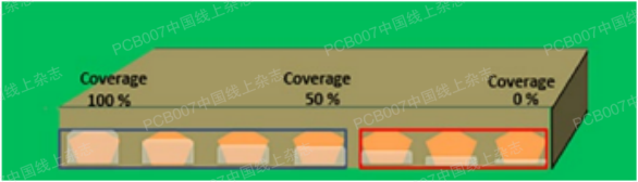
Figure 1 – Pre-treatment and Tin Plating Process of QFN Flanks: (a) After QFN Singulation; (b) After Cleaning and Micro-etching; (c) After Tin Plating
After pre-cleaning, the copper surface appears smooth; scratches and coating contaminants caused by the singulation process are removed. During the immersion tin plating process, the package flanks are covered with immersion tin, forming a dense tin layer that fully covers the side pads of the QFN. Following the tin plating process, post-plating treatment can be applied to prevent discoloration of the tin layer during subsequent assembly, form a hydrophobic surface, and protect the surface from steam aging.
To verify that the tin layer improves solder wetting and enables the formation of three-dimensional solder joints, QFN test samples are immersed in liquid solder for testing to evaluate the surface coverage of the side pads by solder. The samples are immersed in solder at a 45° angle for 5 seconds. Thermal pre-aging tests are performed on the samples at 150°C for 8 hours and 16 hours, followed by steam aging tests at 93°C for 4 hours and 8 hours. Figure 2 shows the acceptance criteria for solder wetting on QFN flanks. Figure 3 presents the performance comparison between the dedicated immersion tin process for QFN plating and the standard PCB immersion tin process applied to QFN packages.
Figure 2 – Acceptance Criteria for Solder Wetting on QFN Flanks
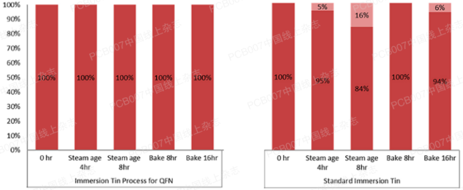
Figure 3 – Solder Wetting Performance of QFN Flanks with Different Immersion Tin Coatings
Solder coverage on the pads must reach at least 50% to be acceptable; coverage below 50% is rejectable. Figure 4 shows example images of soldered flanks. The figure displays soldered pads after baking at 150°C for 16 hours and storage at 93°C with 93% relative humidity for 8 hours.
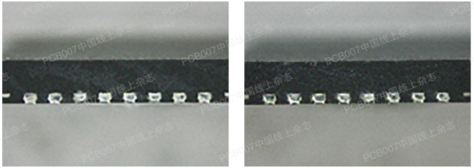
Figure 4 – Example Images of Solder Wetting (Left: After Baking at 150°C for 16 Hours; Right: After Storage at 93°C/93%RH for 8 Hours)
The results confirm that the immersion tin process designed for QFN flanks offers significant advantages over the PCB immersion tin process used for QFN packages in terms of solderability.
During the aging of the immersion tin coating, the thickness of intermetallic compounds (IMCs) increases, leading to a reduction in free tin content; this is critical for the solderability of the tin surface.
Storage tests are conducted to investigate the growth of intermetallic compounds over time with different base alloys. For this test, tin layers are deposited on EFTEC 64T and C194 alloys. The compositions of these two alloys are shown in Table 1.
[Table Position 1: Table 1 – Mass Fraction of Alloys (%)]
| Alloy |
Cu |
Cr |
Sn |
Zn |
Fe |
| EFTEC-64T |
99.25 |
0.3 |
0.25 |
0.2 |
– |
| C194 |
Min. 97 |
– |
– |
0.05~0.20 |
2.10~2.60 |
For all conditions, the total thickness of the deposited tin layer is 1.5 µm. Thermal aging and steam aging tests are performed at 150°C and at 93°C with 93% relative humidity, respectively. The results of IMC and free tin thicknesses are shown in Figure 5, with thicknesses in µm (light blue: free tin; dark blue: IMC).
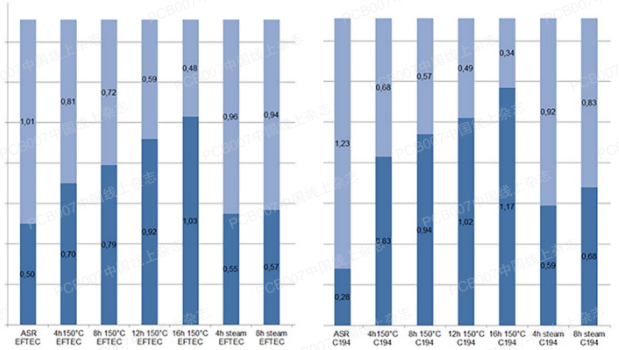
Figure 5 – Results of IMC and Free Tin Thicknesses
The results indicate that the formation of IMCs is primarily influenced by temperature. At a storage temperature of 150°C, the increase in IMCs grows linearly with time. After 4 hours of storage at 150°C, approximately half of the tin thickness is consumed by IMC formation.
During humidity aging at 93°C, IMC formation proceeds at a slower rate, with only about 40% of the tin layer converted to IMCs within the same duration. It is also shown that even after 16 hours of storage at 150°C, 25%~32% free tin remains, ensuring good solderability.
The alloy material has a minimal impact on the coating, resulting in an approximately 10% increase in free tin on EFTEC 64T material.
The tin deposit on the flanks exhibits excellent solderability even after thermal aging or steam aging, with the specific results correlated to whether sufficient free tin remains after IMC formation.
Examination of the effects of various process steps on electrolytic tin deposition on the bottom pads of QFN packages reveals no negative impacts. Tin whiskers are a known risk for immersion tin deposits. To prevent tin whisker formation, an anti-whisker additive is incorporated, which deposits at the grain boundaries of the tin layer and inhibits the formation of tin whiskers.
About Maxipcb
Maxipcb empowers innovators to turn cutting-edge technologies into reality.
We offer one-stop solutions for design, simulation, testing, PCB manufacturing, component procurement and SMT assembly, enabling efficient development, rapid deployment and risk control across the full product lifecycle.Serving the world in communications, industrial automation, aerospace, automotive, semiconductor and beyond, we build a safer, more connected future together.
