Electromagnetic Interference (EMI) has always been the focus of attention for electronic devices and a headache for engineers.
To this day, Electromagnetic Interference (EMI) has always been the focus of attention for electronic devices and a headache for engineers. It threatens the safety, reliability and stability of electronic devices. To improve EMI, reasonable PCB layout is crucial. In this article, I will introduce how to improve EMI through PCB layout to meet customer needs.
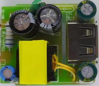
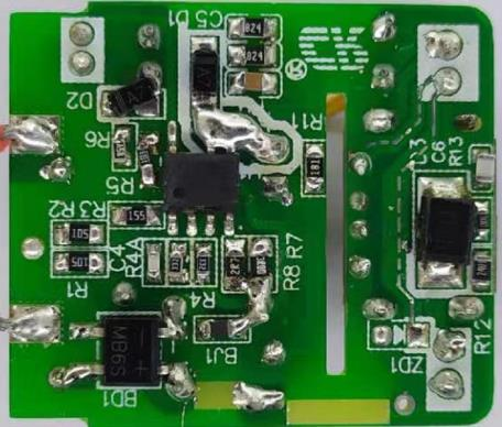
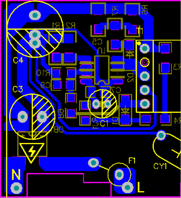
The following is the picture of the test prototype:
【Application】Alternative to linear regulators and RCC / Christmas lights, LED drivers / low-power power adapters / cellular phone chargers
【Specifications】5V1A
【Control IC】CR5215SC
About CR5215SC — High-Precision Constant Current/Constant Voltage Primary-Side Control Power Switch
CR5215SC is a high-performance offline Pulse Width Modulation (PWM) controller applied to low-power AC/DC chargers and power adapters. The chip adopts a primary-side detection and regulation topology, so there is no need for TL431 and optocoupler in application. The chip has built-in constant current and constant voltage control modes.
In constant current control, the maximum output current and output power can be set by the current limiting resistor RS of the CS pin. In constant voltage control, the built-in constant voltage sampling circuit and high-precision error comparator reference voltage ensure the high performance and high precision of the chip. In addition, the built-in line loss compensation circuit ensures the output voltage accuracy from no-load to full-load conditions. The chip also has an extremely low static operating current, and the standby power consumption of the chip is less than 75mW.
CR5215SC has designed a series of perfect protection measures for various faults, including cycle-by-cycle peak current limiting, VDD overvoltage protection, FB open circuit protection, output short circuit protection, leading edge blanking, over temperature protection, power clamp and undervoltage lockout functions. It can effectively protect under fault conditions such as FB pull-up resistor open circuit, FB pull-down resistor short circuit, output diode open circuit or short circuit, transformer winding short circuit, CS pin resistor open circuit, etc., making the chip more reliable.
Main Features
● Low startup current
● Constant voltage accuracy up to ±5%, constant current accuracy up to ±5%
● High-precision constant voltage and constant current output in the full voltage range
● Dynamic load response function
● Programmable CC/CV mode control
● High-efficiency QR control mode
● Built-in primary inductance deviation compensation function
● Built-in output line voltage compensation function
● Built-in full-voltage power adaptive compensation function
● No audio noise control technology
● VDD terminal overvoltage and undervoltage protection functions
● VDD terminal clamp circuit
● Built-in output overvoltage protection function
● Built-in FB open circuit and short circuit protection functions
● Built-in output diode open circuit and short circuit protection functions
● Built-in leading edge blanking circuit
● Cycle-by-cycle current limiting
● Overload protection function
● Over temperature protection function
● SOP-7L green package
Basic Applications
● Low-power power adapters
● Cellular phone chargers
● Christmas lights, LED drivers
● Alternative to linear regulators and RCC
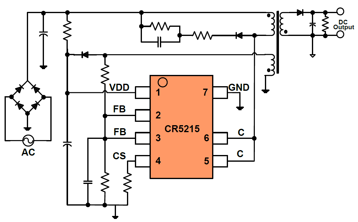
Typical Application
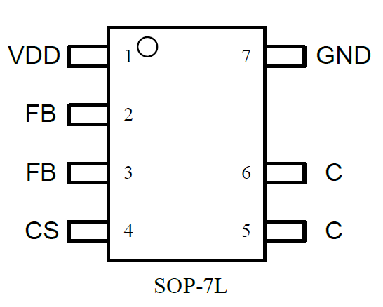
Pin Arrangement
Pin Description
| Pin No. |
Symbol |
Description |
| 1 |
VDD |
Power supply. |
| 2, 3 |
FB |
Auxiliary winding voltage feedback input terminal. This pin is connected to the auxiliary winding that reflects the output voltage through a resistor divider. |
| 4 |
CS |
Current detection input terminal. |
| 5, 6 |
C |
Built-in BJT collector terminal. |
| 7 |
GND |
Ground. |
Problem Description
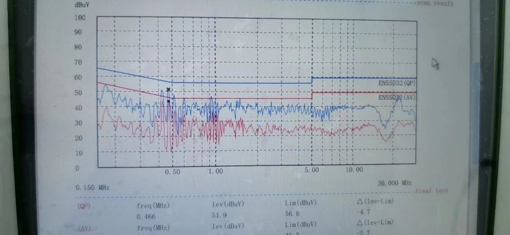
The EMI failed to meet the requirements during the test, and the PCB layout needs to be redone.
Solution Ideas
-
Arrange sensitive components such as switching devices, output inductors and output capacitors in positions where EMI interference is likely to be low. For example, the control signal lines of the switching tube and output inductor should be far away from other signal lines, and the spatial distance from the load terminal should be as short as possible to reduce the length and area of the current loop and lower radiated interference.
-
Install EMI suppression circuits such as filters (e.g., LC filters, Pi filters) directly at the output terminal of the switching power supply. This can effectively reduce signal reflection at the output terminal and increase the efficiency of the filter.
-
Control the switching speed of switching devices. Reducing the switching speed of switching devices, especially in the high frequency band, can effectively reduce the EMI interference generated by the switching power supply.
-
For high-frequency signal traces, adopt the return plane reduction technology, that is, form infinitely small high-frequency loops between the signal lines and the ground lines as much as possible, reduce the loop area of high-frequency signals, and reduce electromagnetic radiation and improve anti-interference ability.
-
For the input signals of the switching power supply, such as AC or DC input, pay attention to using filter capacitors, magnetic beads, etc. for suppression to enhance the anti-interference ability of the switching power supply.
-
Reasonable pin layout. For sensitive pins such as switching tubes, output inductors and capacitors, the shortest possible lead-out method can be adopted to reduce mutual interference between them.
Debugging Key Points
PCB Routing Notes:
-
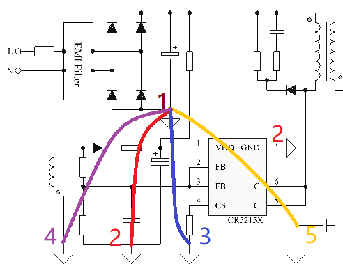
The primary ground connection method should adopt the "star connection method" as much as possible: VDD capacitor ground (including IC-GND, FB lower bias resistor GND), CS sampling resistor ground, transformer auxiliary winding ground, and Y capacitor primary side ground. These four places need to be independently connected to the ground of the primary BUCK capacitor.
-
The trace of the startup resistor should first pass through the "positive terminal of the VDD capacitor" and then connect to the VDD of the IC.
-
The trace of the auxiliary winding power supply loop should first pass through the "positive terminal of the VDD capacitor" and then connect to the VDD of the IC.
-
The VDD capacitor should be as close to the IC terminal as possible.
Note:
- Mark "1" is the primary BUCK capacitor GND;
- Mark "2" are the GND of the IC and the GND of its peripheral devices, which can be connected together through traces;
- Mark "3" is the CS sampling resistor GND;
- Mark "4" is the transformer auxiliary winding GND;
- Mark "5" is the Y capacitor primary side GND.
Final Result
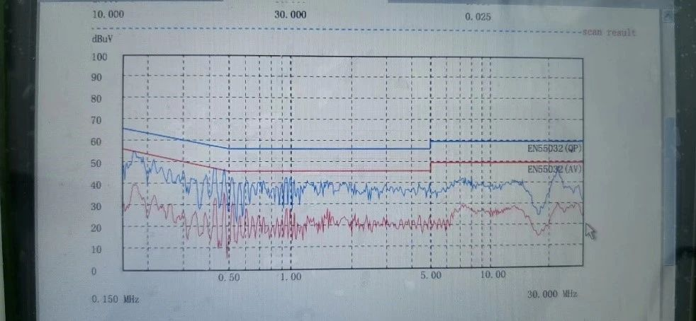
After redoing the PCB layout, the EMI test fully meets the customer's requirements.
About Maxipcb
Maxipcb empowers innovators to turn cutting-edge technologies into reality.
We offer one-stop solutions for design, simulation, testing, PCB manufacturing, component procurement and SMT assembly, enabling efficient development, rapid deployment and risk control across the full product lifecycle.Serving the world in communications, industrial automation, aerospace, automotive, semiconductor and beyond, we build a safer, more connected future together.