I. Differences Between Immersion Gold PCB and Electroplated Gold PCB
| Performance & Surface Plating |
Appearance |
Solderability |
Signal Transmission |
Quality |
Engineering |
| Electroplated Gold PCB |
Gold with whitish tint |
Average, occasional poor soldering |
Skin effect is unfavorable for high-frequency signal transmission |
1. Gold surface is prone to oxidation
2. Easy to cause gold wire micro-short circuit
3. Poor solder mask adhesion |
Line width compensation affects trace spacing |
| Immersion Gold PCB |
Bright golden yellow |
Excellent |
Skin effect has no impact on signals |
1. Not easy to oxidize
2. No gold wire generation
3. Excellent solder mask adhesion |
Line width compensation has no impact on trace spacing |
II. Why Use Electroplated Gold PCB
With the increasing integration of ICs, IC pins are becoming more numerous and finer. The vertical hot air solder leveling (HASL) process is difficult to flatten fine pads, which brings difficulties to SMT mounting. In addition, the shelf life of HASL boards is very short. Electroplated gold PCBs exactly solve these problems:
- For surface mount technology, especially for ultra-small SMD packages of 0603 and 0402, the flatness of the pad is directly related to the quality of the solder paste printing process, and plays a decisive role in the subsequent reflow soldering quality. Therefore, full-board electroplated gold is commonly used in high-density and ultra-small SMD processes.
- In the trial production stage, affected by factors such as component procurement, the boards are often not soldered immediately upon arrival, but are usually used after several weeks or even a month. The shelf life of electroplated gold PCBs is many times longer than that of lead-tin alloy boards, so everyone is willing to adopt them. Furthermore, the cost of electroplated gold PCBs in the sample stage is almost the same as that of lead-tin alloy boards.
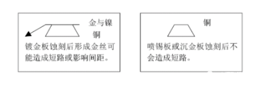
However, with the increasingly dense routing, the line width and spacing have reached 3-4mil, which brings the problem of gold wire short circuit:
- After etching, the gold wires formed on electroplated gold PCBs may cause short circuits or affect trace spacing.
- No short circuit will be formed after etching on HASL boards or immersion gold PCBs.
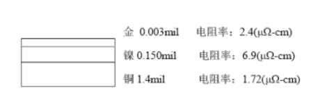
As the signal frequency gets higher and higher, the impact of signal transmission in multi-plating layers caused by the skin effect on signal quality becomes more significant.
Power Union
Skin effect refers to the phenomenon that for high-frequency alternating current, the current tends to concentrate and flow on the surface of the conductor.
According to calculations, the skin depth is related to frequency, as shown in the table below:
| Frequency (Hz) |
Depth (mil) |
Frequency (Hz) |
Depth (mil) |
Frequency (Hz) |
Depth (mil) |
| 60 |
8.6 |
100 |
6.6 |
1k |
2.1 |
| 10k |
0.66 |
100k |
0.21 |
1M |
0.066 |
| 10M |
0.021 |
100M |
0.0066 |
1G |
0.0021 |
Power Union
Other disadvantages of electroplated gold PCBs are listed in the comparison table of differences between immersion gold PCBs and electroplated gold PCBs.
III. Why Use Immersion Gold PCB
To solve the above problems of electroplated gold PCBs, PCBs using immersion gold process have the following main characteristics:
- Due to the different crystal structures formed by immersion gold and electroplated gold, immersion gold presents a more bright golden yellow color than electroplated gold, which achieves higher customer satisfaction.
- Due to the different crystal structures formed by immersion gold and electroplated gold, immersion gold has better solderability than electroplated gold, and will not cause poor soldering and customer complaints.
- Since only the pads on the immersion gold PCB have nickel-gold plating, the signal transmission in the skin effect occurs in the copper layer, which has no impact on the signal.
- The crystal structure of immersion gold is denser than that of electroplated gold, so it is less prone to oxidation.
- Since only the pads on the immersion gold PCB have nickel-gold plating, no gold wire will be generated to cause micro-short circuits.
- Since only the pads on the immersion gold PCB have nickel-gold plating, the adhesion between the solder mask on the circuit and the copper layer is stronger.
- Line width compensation in engineering will not affect the trace spacing.
- Due to the different crystal structures formed by immersion gold and electroplated gold, the stress of the immersion gold PCB is easier to control, which is more conducive to the bonding processing for products with bonding requirements. At the same time, precisely because immersion gold is softer than electroplated gold, immersion gold PCBs are not wear-resistant when used as gold fingers.
About Maxipcb
Maxipcb empowers innovators to turn cutting-edge technologies into reality.
We offer one-stop solutions for design, simulation, testing, PCB manufacturing, component procurement and SMT assembly, enabling efficient development, rapid deployment and risk control across the full product lifecycle.Serving the world in communications, industrial automation, aerospace, automotive, semiconductor and beyond, we build a safer, more connected future together.
- The flatness and shelf life of immersion gold PCBs are as good as those of electroplated gold PCBs.