The purpose of this document is to help users understand how to design a good PCB layout with excellent noise reduction performance. After implementing the countermeasures mentioned in this document, a comprehensive system evaluation is necessary. This document provides instructions based on the RL78/G14 sample board.
The purpose of this document is to help users understand how to design a good PCB layout with excellent noise reduction performance. After implementing the countermeasures mentioned in this document, a comprehensive system evaluation is necessary. This document provides instructions based on the RL78/G14 sample board.
Description of the Test Board
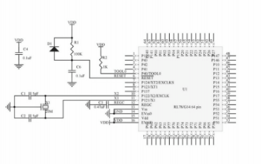
This section presents examples of recommended layouts. All non-recommended boards are fabricated using the same schematic diagram and components, with only the PCB layout differing. Through the recommended methods, the recommended PCB board can achieve higher noise reduction performance. Both the recommended and non-recommended layouts are designed based on the same schematic. Figure 1 shows the circuit schematic around the MCU.
PCB Layouts of the Two Test Boards
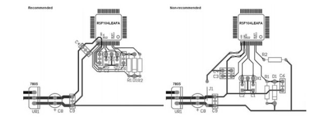
This section shows examples of the recommended layout and the non-recommended layout. The PCB layout should be designed in accordance with the recommended layout to achieve superior noise reduction performance. The reasons for recommending the PCB layout on the left side of Figure 1 will be explained in the next section. Figure 2 shows the PCB layouts around the MCU of the two test boards.
Main Differences Between the Recommended and Non-Recommended Layouts
This section describes the main differences between the recommended layout and the non-recommended layout.
-
Wiring of VDD and VSS
On the recommended board, the VDD and VSS wiring is separated from the peripheral power wiring at the main power inlet. Additionally, the VDD and VSS wiring on the recommended board is closer together than on the non-recommended board. In particular, on the non-recommended board, the MCU's VDD wiring is connected to the main power supply through jumper J1 and then passes through filter capacitor C9.
-
Oscillator Issues
The oscillator circuit (X1, C1, and C2) on the recommended board is placed closer to the MCU than on the non-recommended board. The wiring from the oscillator circuit to the MCU on the recommended board is shorter than on the non-recommended board. On the non-recommended board, the oscillator circuit is not located at the terminal of the VSS wiring and is not separated from other VSS wiring.
-
Bypass Capacitors
The bypass capacitor C4 on the recommended board is placed closer to the MCU than on the non-recommended board, and the wiring from the bypass capacitor to the MCU is shorter. In particular, on the non-recommended board, the leads of C4 are not directly connected to the VDD and VSS main lines.
About Maxipcb
Maxipcb empowers innovators to turn cutting-edge technologies into reality.
We offer one-stop solutions for design, simulation, testing, PCB manufacturing, component procurement and SMT assembly, enabling efficient development, rapid deployment and risk control across the full product lifecycle.Serving the world in communications, industrial automation, aerospace, automotive, semiconductor and beyond, we build a safer, more connected future together.