Impedance is familiar to all engineers, but few can explain it clearly. It seems simple but is actually difficult to articulate.
Impedance is familiar to all engineers, but few can explain it clearly. It seems simple but is actually difficult to articulate.
Below, we will help you master impedance easily through a quick Q&A format!
Q01: What is Impedance?
A: In circuits containing resistance, inductance, and capacitance, the opposition to alternating current is called impedance, commonly denoted as Z. Impedance consists of resistance, inductive reactance, and capacitive reactance, but it is not a simple sum of the three. The unit of impedance is the ohm (Ω).
Impedance in PCBs refers to the electrical impedance between conductors, power supplies, loads, and other components on the circuit board. PCB impedance control is a critical step in designing printed circuit boards to ensure board performance and stability. In high-speed circuit design, maintaining proper impedance is essential, as improper impedance will cause severe noise interference to signals.
Q02: What is Single-Ended Impedance?
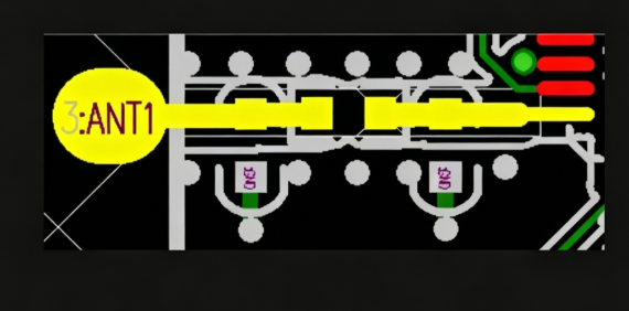
A: Single-ended impedance is a type of characteristic impedance, referring to the impedance of a single signal line in a circuit. In single-ended transmission, signals are transmitted through a single signal line.
Q03: What is Differential Impedance?
A: The differential signal line structure is used for impedance control. The driving end inputs two signal waveforms with opposite polarities, which are transmitted through two differential lines, and the receiving end performs subtraction processing. This method is used in high-speed digital-analog circuits to improve signal integrity and anti-noise interference capability.
Q04: What is Coplanar Impedance?
A: Coplanar impedance is the test impedance when a signal line transmits between GND/VCC planes. Coplanar waveguide is a common planar structure conductor line in high-frequency and microwave circuits. Coplanar impedance is related to factors such as the waveguide geometry, conductor width, and dielectric parameters. By adjusting these factors, the propagation characteristics of electromagnetic waves in the coplanar waveguide can be controlled. The magnitude of coplanar impedance determines the propagation characteristics of electromagnetic waves in the coplanar waveguide.
Q05: Why is Single-Ended Impedance Controlled at 50 Ohms?
A: 50 ohms is the industry default value, offering advantages of easy processing and low loss, but it is not mandatory. It depends on the interface: for example, 75 ohms is the standard for long-distance communication, and PCB line impedance must be matched when cables and antennas use 75 ohms. Special chips can reduce impedance by improving driving capability, enhancing EMI and crosstalk suppression effects. For instance, Intel requires impedance control at 37 ohms, 42 ohms, or even lower.
Q06: Why is Differential Impedance Controlled at 100 Ohms?
A: The setting of differential and single-ended impedance has certain historical evolution and application background. These impedance values are mainly determined to meet the requirements of specific interfaces and chips, ensuring stable signal transmission and good electrical performance. The common impedance value is 100 ohms, and there are also 90 ohms and 85 ohms. These impedance settings can reduce signal reflection, interference, and distortion, improving signal transmission efficiency.
Q07: Why Should Differential Lines Be Routed in Parallel?
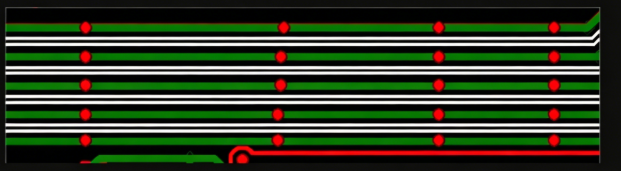
A: Differential lines are usually designed with parallel routing to improve anti-interference capability and maintain impedance continuity. This design keeps the coupling degree between the two lines unchanged, ensuring impedance continuity.
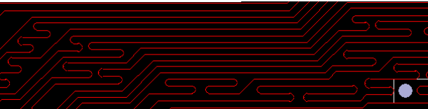
However, the definition of differential lines does not require parallel routing. When non-parallel routing is adopted, it is necessary to ensure that the spacing is greater than 5W, the single-line impedance is consistent, and external interference is minimal. This allows non-parallel routing without coupling the two lines.
In test fixtures, differential lines are usually single-ended routed with impedance controlled at 50 ohms. Using flying wires or coaxial cables to connect the two lines can also achieve differential transmission as long as they finally converge to the receiving end.
Q08: Can Differential Lines Be Unequal in Length?
A: No. Equal length is the most important physical rule for differential lines.
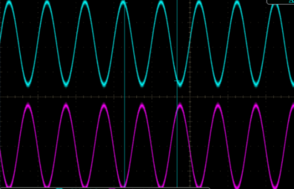
Equal length of differential lines is crucial because the receiving end performs a difference operation on the signals of the two lines. Signals are trapezoidal waves, and unequal length lines will cause phase errors, which may lead to transmission errors. The ideal signal should have peaks aligned with troughs, but unequal length lines may cause a phase difference of up to 180 degrees, resulting in transmission errors.
Even a small phase difference, such as 30 degrees, will seriously degrade the eye diagram, convert differential-mode components into common-mode components, and reduce common-mode immunity. Therefore, equal length of differential lines is a key indicator, usually requiring an error of no more than 5mil, with a maximum allowable error of 10mil.
Q09: Can Differential Pairs Be Routed on Different Layers?
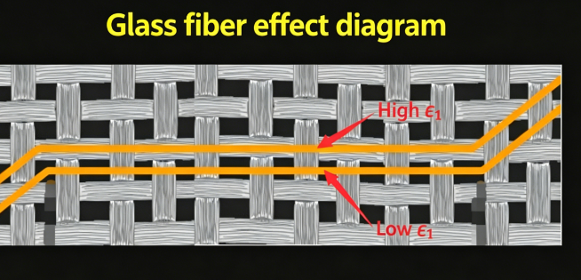
A: Yes, routing on upper and lower layers is possible, and theoretically this method is superior to same-layer routing. First, it facilitates BGA breakout. More importantly, distributing differential lines on different layers can greatly reduce the impact of the glass weave effect.
However, in practical engineering, due to manufacturing process limitations, random errors may occur in routing on different layers, resulting in inaccurate overlap of the upper and lower layer traces. This error may seriously affect the performance of differential lines, so this routing method has certain drawbacks.
Q10: What Factors Affect Impedance in High-Speed PCB Design?
A:
- Trace Width: Impedance is inversely proportional to trace width; narrower traces result in higher impedance, while wider traces result in lower impedance.
- Copper Foil: Impedance is inversely proportional to copper foil thickness; thicker copper results in lower impedance, while thinner copper results in higher impedance.
- Trace Spacing: Impedance is directly proportional to spacing; larger spacing results in higher impedance, while smaller spacing results in lower impedance.
- Coplanar Conductors: Impedance is directly proportional to the distance between the impedance line and coplanar conductors; larger distance results in higher impedance, while smaller distance results in lower impedance.
Q11: What Factors in PCB Fabrication and Material Selection Affect Impedance?
A:
- Dielectric Thickness: Impedance is directly proportional to dielectric thickness; thicker dielectric results in higher impedance, while thinner dielectric results in lower impedance.
- Dielectric Constant (Dk): Impedance is inversely proportional to dielectric constant; higher Dk results in lower impedance, while lower Dk results in higher impedance.
- Solder Mask Thickness: Impedance is inversely proportional to solder mask thickness within a certain range; thicker solder mask results in lower impedance, while thinner solder mask results in higher impedance.
About Maxipcb
Maxipcb empowers innovators to turn cutting-edge technologies into reality.
We offer one-stop solutions for design, simulation, testing, PCB manufacturing, component procurement and SMT assembly, enabling efficient development, rapid deployment and risk control across the full product lifecycle.Serving the world in communications, industrial automation, aerospace, automotive, semiconductor and beyond, we build a safer, more connected future together.