Daily activities such as walking and dressing cause friction that generates static voltages of varying amplitudes. However, the energy is too low to harm the human body. For electronic components, this static energy cannot be ignored.
Daily activities such as walking and dressing cause friction that generates static voltages of varying amplitudes. However, the energy is too low to harm the human body. For electronic components, this static energy cannot be ignored.
In dry environments, the voltage of human-body static electricity (ESD) can easily exceed 6–35 kV. Touching electronic devices, PCBs, or components on a PCB by hand may cause instantaneous electrostatic discharge, interfering with or even damaging the devices or PCB components.
The figure below lists the static voltage levels generated by different daily activities:
| Activity Mode |
Static Voltage / kV (10%–20% RH) |
Static Voltage / kV (65%–90% RH) |
| Walking on a carpet |
35 |
1.5 |
| Walking on a vinyl resin floor |
12 |
0.25 |
| Working at a workbench |
6 |
0.1 |
| Opening ethane resin packaging |
7 |
0.6 |
| Picking up an ordinary polyethylene bag |
20 |
1.2 |
| Sitting on a polyurethane foam chair |
18 |
1.5 |
How Static Electricity Is Generated
Static electricity is a form of electrical energy that exists on the surface of objects. It occurs due to local imbalance between positive and negative charges. For example, contact electrification (triboelectric effect) is a typical electrostatic discharge phenomenon.
Static electricity has long plagued many electronic products. The electromagnetic fields generated by discharge currents cause severe interference to circuits through capacitive coupling, inductive coupling, or spatial radiation coupling. Therefore, electrostatic protection must be considered in the early stage of PCB design.
The figure below is a schematic diagram of static electricity generation:
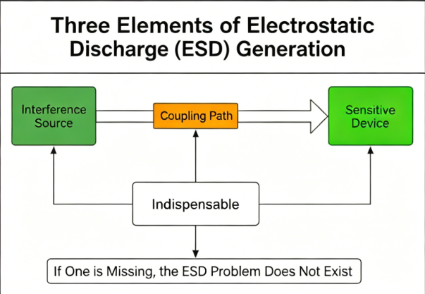
Three Key Elements of Static Electricity (ESD) Generation
- Interference Source
- Coupling Path
- Sensitive Equipment
All three are indispensable; the absence of any one eliminates ESD issues.
How to Design PCBs for ESD Protection
The basic principle of PCB layout is to place ESD protection components as close as possible to input terminals or connectors. The trace length between ESD protection components and the protected lines shall be minimized.
For PCB design, setting a proper isolation distance at edges prone to ESD events is critical. For chassis-based products, the breakdown distance is approximately 1 mm per 1 kV of static voltage. A 3–5 mm isolation zone at discharge-prone edges can withstand 3–5 kV static voltage.
1. ESD Protection Design for Low-Speed PCBs
- Route traces horizontally and vertically, and minimize parallel routing of signal lines.
- Use wider traces if space permits.
- Apply high-speed circuit design principles for routing.
- Avoid routing critical signals (e.g., clock, reset signals) near PCB edges.
- Minimize all conductive loops on the PCB, including power and ground loops.
- For single or double-sided PCBs without a power plane, a ground trace must run alongside every power trace.
- Use multilayer PCBs whenever possible.
2. ESD Protection Design for High-Speed PCBs
- Ensure traces have a robust ground plane reference.
- Maintain sufficient spacing between filters, optocouplers, AC power lines, and weak signal lines.
- Add low-pass filters (capacitors, ESD devices, RC, LC networks) for long-distance traces.
- Implement isolation (add shielding covers) and avoid parallel routing between protected and unprotected conductors.
- Do not share a common ground return path with other devices.
3. General Methods for ESD Prevention
- Maintain a complete ground structure, enlarge the static discharge area, apply uniform copper pouring, keep ground resistance stable, and ensure flat and stable ground planes.
- Implement a perimeter ground ring around the PCB and surround data lines with ground copper.
- Use as many ground vias as possible to tightly connect ground planes across all layers.
- Install optocouplers or transformers on the PCB, combined with dielectric isolation and shielding, to effectively suppress ESD surges.
- Connect the PCB GND to the chassis ground at a single point (preferably at the cable entry) to prevent ESD currents on the chassis from coupling into the circuit.
- If PCB area allows and the overall system bonding and static discharge paths are reliable, add a grounded protection ring around the PCB (bare copper, with multiple vias to ground).
We have shared key ESD protection practices. Below is a recommended DFM and assembly analysis tool to detect potential risks in PCB design and identify defects before production, helping engineers optimize hardware design.
About Maxipcb
Maxipcb empowers innovators to turn cutting-edge technologies into reality.
We offer one-stop solutions for design, simulation, testing, PCB manufacturing, component procurement and SMT assembly, enabling efficient development, rapid deployment and risk control across the full product lifecycle.Serving the world in communications, industrial automation, aerospace, automotive, semiconductor and beyond, we build a safer, more connected future together.
