As an NPI engineer, DFM (Design for Manufacturability) analysis covers a wide range of aspects, which is highly relevant to today’s topic—PCB assembly design techniques. This article focuses on PCB Assembly Design (DFA, Design for Assembly) and practical tips for PCB assembly design.
As an NPI engineer, DFM (Design for Manufacturability) analysis covers a wide range of aspects, which is highly relevant to today’s topic—PCB assembly design techniques. This article focuses on PCB Assembly Design (DFA, Design for Assembly) and practical tips for PCB assembly design.
1. What is PCB Assembly Design (DFA)?
PCB assembly refers to the process of integrating printed circuit boards with other electronic components (such as connectors, housings, heat sinks, etc.) to embed them into the final product.
PCB assembly design means taking PCB assembly into account in the early design stage to achieve an optimal product.
A common mistake, rarely made by experienced PCB designers but frequently by beginners, is failing to fully consider assembly in the initial circuit board design. Instead, excessive attention is paid to the PCB itself without a thorough understanding of manufacturing issues.
Ignoring PCB assembly will lead to a series of consequential problems:
- A PCB design that seems acceptable on its own may cause severe assembly issues, such as excessively close spacing between components, resulting in product malfunction or performance degradation.
- Component availability issues: if components are unavailable, the entire manufacturing process will be delayed.
To avoid such errors, experienced PCB Layout engineers follow 18 practical PCB assembly design tips as summarized below.
2. PCB Assembly Design Tips
1. Pay Attention to Component Clearance
One of the most common concerns raised by senior PCB Layout engineers is component-to-component spacing.
Excessively close placement between components triggers various issues, which may require redesign and remanufacturing, leading to time and cost losses.
Senior PCB Layout engineers typically reserve sufficient clearance between component boundaries to mitigate potential risks caused by tight component placement.
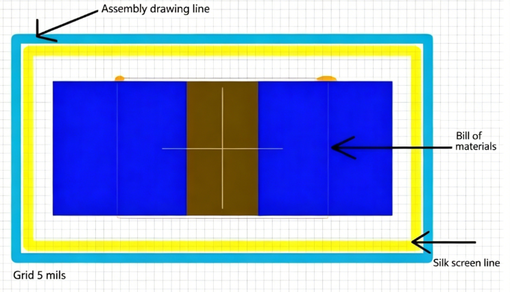
Component Placement Around Silkscreen and Assembly Lines

Component Spacing Diagram
PCB Layout engineers must carefully place components to prevent overlapping outlines. As shown in the diagram, a spacing of 50 mils is maintained between components.
General layout and routing rules specify that the minimum spacing between discrete components such as capacitors and resistors shall be at least 10 mils, with 30 mils as the preferred spacing. Additional spacing specifications are listed in the table below (values for reference only, subject to actual conditions).
Component Spacing Values (Unit: mil)
|
Chip |
SOT |
SOIC |
PLCC |
QFP |
BGA |
Axial |
PTH Conn |
| Chip |
10-20 |
15-25 |
20-25 |
50-75 |
50-120 |
75-120 |
50-75 |
50-75 |
| SOT |
15-25 |
15-25 |
20-25 |
50-75 |
50-120 |
75-120 |
50-75 |
50-75 |
| SOIC |
20-25 |
20-25 |
30-50 |
50-100 |
75-120 |
75-120 |
50-75 |
100-150 |
| PLCC |
50-75 |
50-75 |
50-100 |
100-120 |
100-120 |
100-120 |
100-150 |
100-150 |
| QFP |
50-120 |
50-120 |
75-120 |
100-120 |
100-120 |
75-120 |
100-150 |
100-150 |
| BGA |
75-120 |
75-120 |
75-120 |
100-120 |
75-120 |
100-120 |
100-150 |
100-150 |
| AXIAL |
50-75 |
50-75 |
50-75 |
100-150 |
100-150 |
100-150 |
100-150 |
100-150 |
| PTH Conn |
50-75 |
50-75 |
100-150 |
100-150 |
100-150 |
100-150 |
100-150 |
100-150 |
2. Select Components in the Design Stage
Experienced PCB Layout engineers select components at the early design stage to avoid major conflicts between design and actual assembly.
Considering component dimensions and space upfront minimizes assembly issues.
Smaller components occupy less PCB area; evaluate whether component size can be reduced accordingly.
3. Separate Leaded and Lead-Free Components
Never mix lead-free and leaded components. If any assembly requires lead-free processing and no alternative conventional leaded solder is available, the entire PCB must be lead-free assembled, and all components must comply with lead-free assembly requirements.
In some cases, the only available package for a specific device is lead-free BGA, which is subject to specific application requirements.
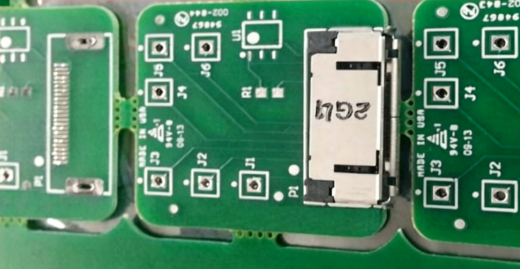
Separation Strips Between PCBs Interfering with Edge Connectors
Separation strips remaining between PCBs after routing may interfere with connectors extending to the board edge. Such issues arise due to poor coordination between PCB manufacturing and assembly.
4. Distribute Large Components Uniformly
Distribute large components as evenly as possible across the PCB during layout to achieve optimal thermal distribution during reflow soldering. Confirm that the PCB manufacturer develops a dedicated reflow profile for the assembly.
5. Keep SMD Components Away from PCB Edge
SMD components should be placed at least 150 mils (3.8 mm) from the board edge, especially when V-Cut is applied.
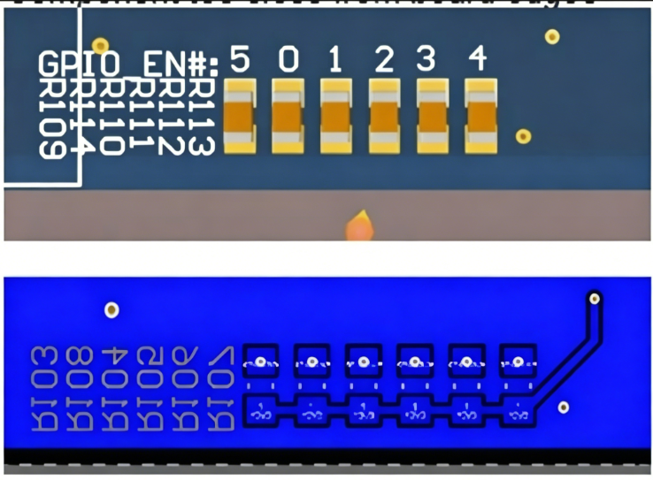
SMD Component Placement Relative to PCB Edge
6. Avoid Using Extremely Small Drill Bits
A 6-mil drill hole is nearly the minimum mechanical drilling size and is not recommended unless no alternative exists. For BGA-density designs, 18.5/8 (18.5 mil pad / 8 mil drill) is suggested; 22/10 is ideal but often not feasible for BGAs (data for reference only, subject to actual conditions).
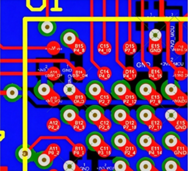
15/6 mil Via Design
7. Maintain Minimum 150 mils Spacing Between SMD and THT Components
This facilitates selective wave soldering or assembly with wave soldering pallets.
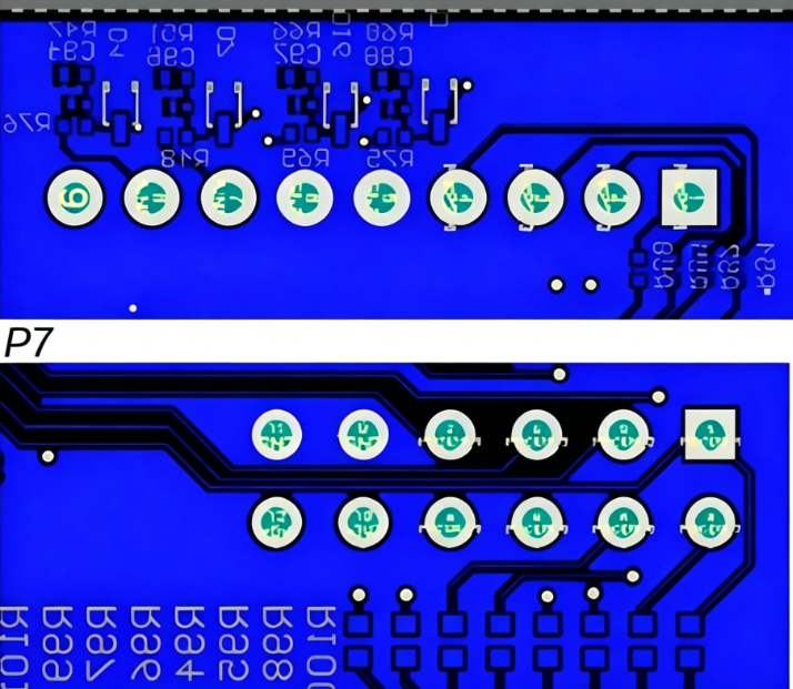
Bottom SMD Components Too Close to TH Vias
8. Correct Definition of Mounting Holes
Mounting holes are typically tool holes defined in the drill drawing with accurate center coordinates and drill diameters. Improper definition (e.g., notches) results in mounting features not being placed on the drilling stage but completed in the low-precision routing stage.
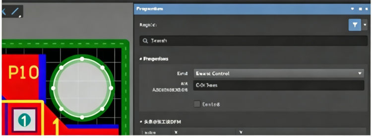
Improperly Defined Mounting Hole
9. Clearance Around Mounting Holes
Sufficient clearance must be maintained around mounting holes if adjacent components are present.
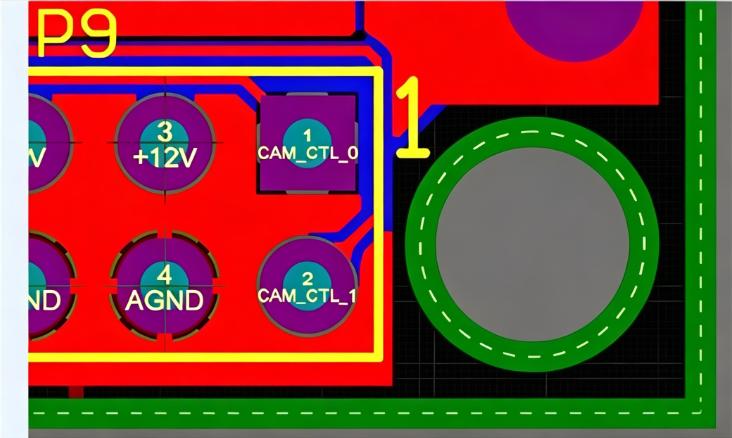
Insufficient Clearance Between Connector Mounting Hole and Adjacent Components
10. Avoid Mixed Manufacturing Processes
Minimize mixed processes. For example, concentrate all through-hole components on the same side of the board to reduce PCB manufacturing and assembly costs and lead time.
11. Select Appropriate Package Sizes
Verify component packages early in layout. If PCB space permits and small packages are unnecessary, use larger packages to simplify PCB assembly.
Example: Prefer 0402 resistors over 0201; use 0805 resistors instead of 1206 if specifications are met, to balance PCB size and assembly.
12. Source Components with Suitable Lead Times
Component availability causes severe production delays. Verify component inventory, lead time, and obsolescence status during the design stage via authorized electronic component platforms.
RC0402FR-07301KL Global Suppliers
Global Suppliers (12)
Currency: RMB (13% VAT)
Demand Quantity: 100
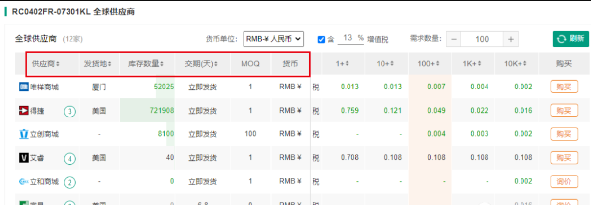
Component Lead Time and Inventory Table
13. Keep BOM Updated During Design
Bill of Materials (BOM) is critical for design and assembly.
Any BOM error will suspend the project at the PCB factory until resolved with the engineer.
Update the BOM simultaneously with design changes: when adding new components to the schematic, refresh the BOM with correct manufacturer part numbers, descriptions, and values.
Engineers often change components due to lead time, size, or availability but forget to update the BOM, causing assembly delays.
A properly formatted BOM includes the following columns:
- Complete Manufacturer Part Number (MPN)
- Manufacturer Name
- Item Number
- Quantity Per Board
- Comma-separated Reference Designators
- Complete Part Description
Optional: Distributor Name, Distributor Part Number
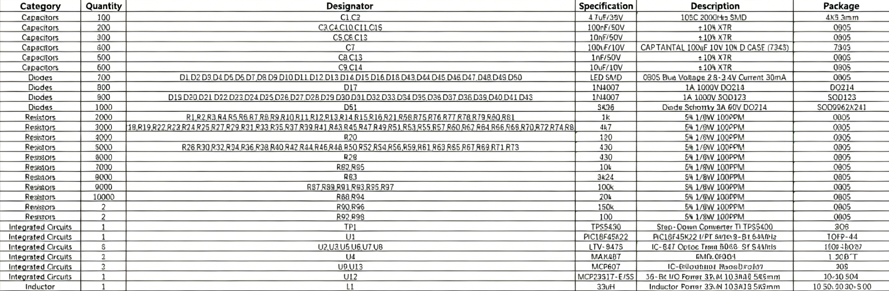
BOM Table Example
14. Verify Component Footprint
Component footprint is another key layout factor.
Correctly use the part number key from the datasheet to identify the correct component and corresponding land pattern. Misinterpreting the datasheet leads to incorrect footprints, requiring full PCB redesign and remanufacturing.
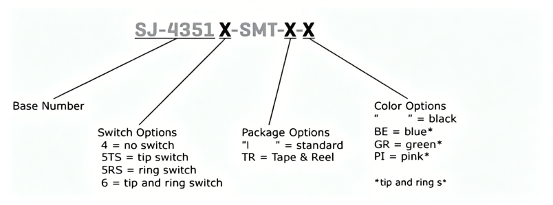
Part Number Key and Package Types Example
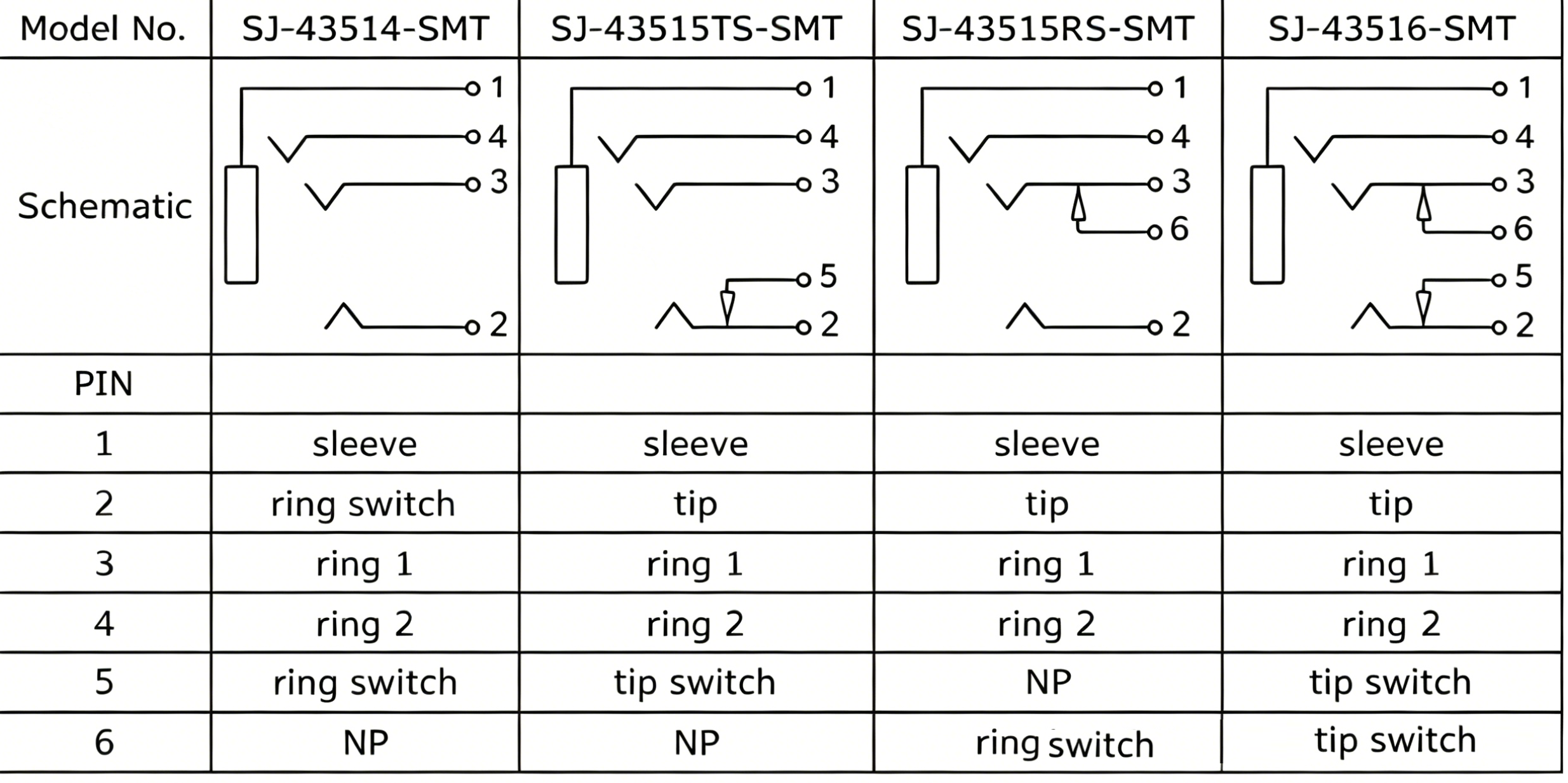
Part Number Key and Pin Configuration Table
15. Ensure All Component Markings Are Present
Missing Pin 1 indicators or component polarity/direction markings on silkscreen is a major assembly roadblock. Nearly 75% of assembly orders received by factories lack clear Pin 1 identification for ICs or misstate/omit polarity markings for capacitors, diodes, or LEDs.
Best practice to avoid assembly issues: Consult the PCB factory before starting design.
- Diode/LED Polarity: Mark the cathode with "K" on the silkscreen, or use the correct diode symbol. Never indicate polarity based on the anode pad.
- Tantalum Capacitor Polarity: Mark the positive electrode with "+" on the silkscreen (reverse polarity may cause ignition).
- Silkscreen must not overlap pads, and symbols shall not be printed under component bodies.
16. Each Component Connection Requires an Independent Pad
Pad dimensions must match the corresponding component. Shared pads (e.g., between a resistor and a capacitor) prevent proper alignment during assembly.
Excessively large pads may cause component tombstoning due to unbalanced solder deposition.
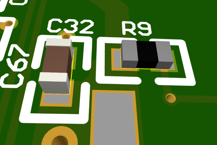
Independent Pads for Each Component
Define properly sized solder mask-defined pads if contact occurs with thermal relief planes. For devices combining non-solder mask-defined pads and solder mask-defined pads (e.g., BGA arrays with loose pitch where outer balls share thermal relief), specify in design notes that the PCB factory shall not edit solder mask apertures for these pads.
17. Material Procurement Management
Many PCB factories provide one-stop services (PCB design, material procurement, stencil & fixture manufacturing, PCBA assembly).
If components are not fully supplied by the factory, provide well-organized kits matching the BOM. All SMT components shall be supplied in reels, continuous tapes (minimum 6 inches), tubes, or trays.
Add spare components for each BOM line item to cover assembly losses (e.g., 10%–20% extra for 0201 1kΩ resistors). Components for each BOM line must be packed in clearly labeled bags and separated from others.
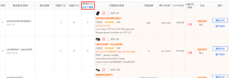
Spare Parts List for One-Stop PCB Factory
All ICs must be shipped in original, unopened protective packaging with desiccants.
Best practice to avoid material issues: Consult the PCB factory before design; one-stop PCBA services are highly recommended.
18. DFM Check
A critical step to ensure error-free and reliable PCB performance is to run Design for Manufacturability (DFM) analysis. DFM testing identifies design errors early, avoiding costly rework and delays in later stages, and effectively detects issues such as component spacing, polarity, and footprint mismatches.
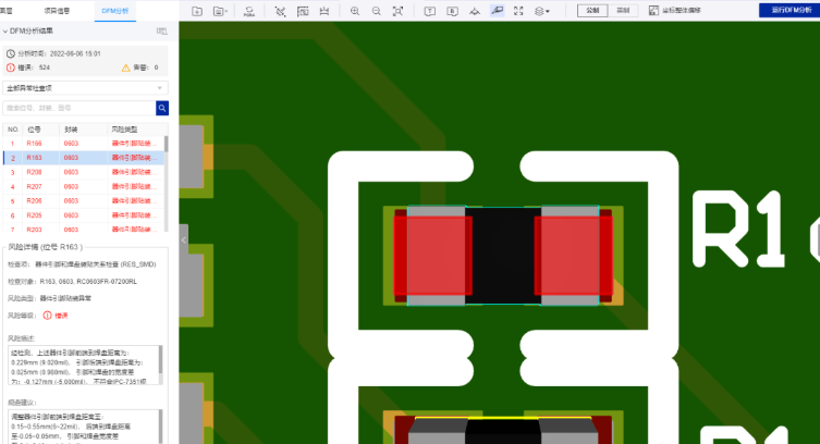
DFM Analysis Interface (Layer, Project Information, DFM Analysis, Offset Settings)

DFM Analysis Report
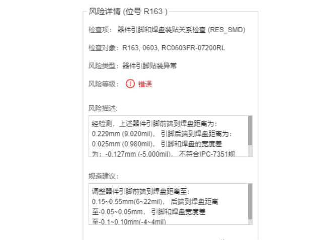
DFM Anomaly List (Ref Des, Package, Risk Type
DFM testing also delivers the following benefits:
- Reduce production costs
- Accelerate delivery and shorten rework time
- Improve product quality
Various DFM analysis software tools are available on the market; details are not repeated here.
About Maxipcb
Maxipcb empowers innovators to turn cutting-edge technologies into reality.
We offer one-stop solutions for design, simulation, testing, PCB manufacturing, component procurement and SMT assembly, enabling efficient development, rapid deployment and risk control across the full product lifecycle.Serving the world in communications, industrial automation, aerospace, automotive, semiconductor and beyond, we build a safer, more connected future together.
