Electronic products such as mobile phones, smart watches, and TWS earphones often need to undergo electrostatic discharge (ESD) testing during certification. In the test, unrecoverable failures or system reset and restart may occur.
Electronic products such as mobile phones, smart watches, and TWS earphones often need to undergo electrostatic discharge (ESD) testing during certification. In the test, unrecoverable failures or system reset and restart may occur.
Detailed Problem Description
A smart watch experiences system reset and even random crashes that cannot recover for a long time when subjected to contact ESD ±4KV on the charging input terminal. The charging terminal is on the bottom layer, and the board is a 4-layer 1-step PCB.
Specific Problem Analysis
- Analysis as follows:
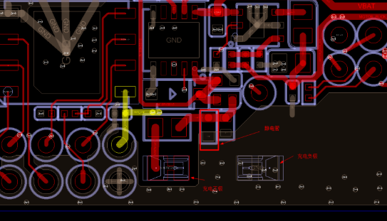
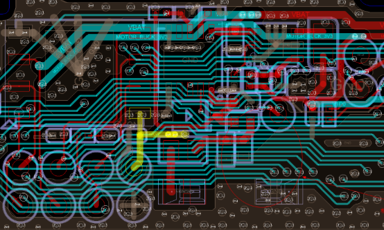
Through the research on the PCB, it is found that there are too many signal traces on the adjacent layer below the charging spring and the positive charging path, without a complete ground plane for ESD discharge, and high-speed flash signals pass through. When ESD strikes, the ESD interferes with the signal traces instantly before the ESD diode can discharge the static electricity, resulting in system abnormality.
Routing of the 4th Layer (Bottom Layer, where the charging contact spring is:
Routing of the 3rd Layer:
- Experiments based on the above analysis
(1) Parallel an ESD diode near the positive spring of the charging input, so that the ESD can be discharged from the ESD diode immediately when the positive contact spring is struck by ±6KV contact ESD.
(2) Suspend the positive spring (to verify whether the bottom layer where the spring is located affects the signal traces on the adjacent layer below the spring), then fly a wire from the positive spring of the charging input to the capacitor at the input terminal of the charging IC, and disconnect the path before the capacitor (to ensure the normal charging path). The purpose is to prevent ESD current from passing through the charging path routing on the original PCB and interfering with the adjacent signal traces. After such treatment, the product passes ±6KV contact ESD test stably without abnormality. By contrast, it fails even at ±3KV without treatment.
Problem Solution
Rectification idea: Optimize PCB layout and routing (remove the signal traces below the ESD path), shorten the charging loop (to shorten the ESD passage path), keep clear and no routing below the charging loop, and provide a complete ground plane on the adjacent layer of the ESD passage path. The ESD discharge path enters the 2nd layer main ground plane through the ground of the 3rd layer.
Specific optimization is as follows:
Optimized PCB Routing
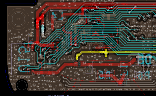
Partial traces are moved to the 2nd layer
The adjacent layer below the ESD loop is a complete ground plane
Summary and Suggestions
ESD has radiation interference. In PCB layout and routing, the ESD diode should be placed as close as possible to the ESD entry point, and vias should be drilled nearby to allow static electricity to enter the main ground plane quickly, so as to avoid interfering with other sensitive devices or traces. The adjacent layers of the ESD passage path should have a complete ground plane as much as possible to avoid passing sensitive signals.
About Maxipcb
Maxipcb empowers innovators to turn cutting-edge technologies into reality.
We offer one-stop solutions for design, simulation, testing, PCB manufacturing, component procurement and SMT assembly, enabling efficient development, rapid deployment and risk control across the full product lifecycle.Serving the world in communications, industrial automation, aerospace, automotive, semiconductor and beyond, we build a safer, more connected future together.