Great importance is attached to signal integrity in current product design, but insufficient attention is paid to power integrity. The main reason is that for low-frequency applications, the design of switching power supplies mostly relies on experience or functional-level simulation assistance, and power integrity analysis seems to be of little help.
Great importance is attached to signal integrity in current product design, but insufficient attention is paid to power integrity. The main reason is that for low-frequency applications, the design of switching power supplies mostly relies on experience or functional-level simulation assistance, and power integrity analysis seems to be of little help. For medium and low-frequency applications within 50MHz to 100MHz, the empirical design rules for capacitors in switching power supplies are sufficient in most cases; even Excel-based tools provided by some chip companies can solve problems in this frequency band.
It is believed that for applications above 100MHz, power integrity issues are basically related to ICs rather than board-level design, so board-level-only power integrity simulation is meaningless unless chip-to-chip solutions combined with package and die models are implemented. Is this really the case?
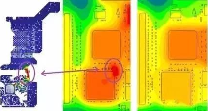
In fact, there is a lot to do in power integrity. The main simulation types in power integrity analysis include DC voltage drop analysis, decoupling analysis, and noise analysis. DC voltage drop analysis involves examining complex traces and plane shapes on the PCB to determine the voltage loss caused by copper resistance.
In addition, it can be used to identify high current density regions. In practice, thermal simulators can be used for co-simulation to observe thermal effects. The solution to DC voltage drop problems is straightforward: add more metal. This additional metal can be in the form of wider and/or thicker traces and planes, extra planes, or additional vias.
The decoupling analysis discussed briefly above aims to determine and minimize the impedance between power and ground at different IC locations on the board.
Decoupling analysis typically drives changes in the value, type, and quantity of capacitors used in the PDN. Therefore, it requires capacitor models including parasitic inductance and resistance. It also drives changes in capacitor mounting methods and/or board layer stack-up to meet low-impedance requirements. There are various types of noise analysis. They may include noise propagating around the board from IC power pins, which can be controlled by decoupling capacitors.
Through noise analysis, the coupling of noise from one via to another can be investigated, and simultaneous switching noise can be analyzed. In many cases, this noise is caused by signal switching (from 1 to 0 and 0 to 1), so it is closely related to signal integrity. In all cases, the ultimate goal of these power integrity analyses is to drive changes to the PDN: power/ground plane pairs, traces, capacitors, and vias.
The PDN not only serves as a means to supply current to ICs but also acts as a return current path for signals. A great deal of overlap between signal integrity and power integrity occurs at vias. For single-ended signals passing through vias, the PDN acts as the return current path for that signal, with nearby vias or capacitors providing paths for the return current to move from one plane to the next. Therefore, the PDN actually determines the impedance and delay characteristics of that single-ended via and is critical for accurate modeling of faster single-ended signals such as DDR3 and DDR4. Using this same combined SI/PI via model, the coupling from one via to the next and the coupling of signals through vias to the PDN can be analyzed.
Similarly, the PDN is critical for minimizing noise that can be caused by multiple signals switching simultaneously (commonly referred to as SSN). If the PDN impedance at the IC power pins is too high, when all drivers switch simultaneously, their switching current will generate voltage fluctuations that can be observed in the signals themselves.
The analysis of signal integrity and power integrity is essential for successful high-speed digital design. It provides valuable insights into what design changes are required. Furthermore, as modeling methods and computing power improve, the ability to simulate both types of integrity simultaneously provides a clear understanding of the actual circuit behavior, the true margins in the design, and how they can achieve optimal performance.
[Table Position 1: Comparison between Signal Integrity and Power Integrity]
|
Signal Integrity |
Power Integrity |
| Became Mainstream |
About 20 years ago |
About 5 years ago |
| Analysis Basis |
Transmission line |
Transmission plane |
| Typical Impedance Target |
~50Ω |
~mΩ |
| Analysis Components |
Signal quality |
DC voltage drop |
| / |
Timing |
Decoupling |
| / |
Crosstalk |
Noise |
| Required Models |
IBIS, SPICE |
Capacitors with parasitics |
| Driven PCB Design Changes |
Trace width |
Amount of current-carrying metal |
| / |
Trace length |
Quantity, value, mounting of capacitors |
| / |
Trace spacing |
Power/ground plane pairs, traces |
Maxipcb empowers innovators to turn cutting-edge technologies into reality.
We offer one-stop solutions for design, simulation, testing, PCB manufacturing, component procurement and SMT assembly, enabling efficient development, rapid deployment and risk control across the full product lifecycle.Serving the world in communications, industrial automation, aerospace, automotive, semiconductor and beyond, we build a safer, more connected future together.