- Pre-divide the routing areas for digital, analog, and DAA signals on the PCB.
- Separate digital and analog components as well as their corresponding traces as much as possible, and place them within their respective routing areas.
- Keep high-speed digital signal traces as short as possible.
- Keep sensitive analog signal traces as short as possible.
- Allocate power and ground reasonably.
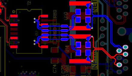
- Separate digital ground (DGND), analog ground (AGND), and protective earth.
- Use wide traces for power and critical signal routes.
- Arrange power and ground traces in a radial pattern as much as possible, and avoid looped routing for signal traces.
- Place digital circuits near parallel bus/serial DTE interfaces, and DAA circuits near telephone line interfaces.
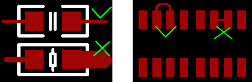
- Traces for small discrete components shall be symmetrical; leads for closely spaced SMT pads shall be connected from the outer side of the pads, and direct connection through the center of the pads is prohibited.
- Priority for critical signal traces: Priority shall be given to critical signals such as power, small analog signals, high-speed signals, clock signals, and synchronization signals.
- Routing density priority principle: Start routing from components with the most complex connection relationships on the board, and begin from the area with the densest wiring on the board.
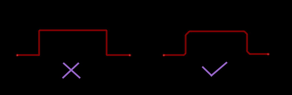
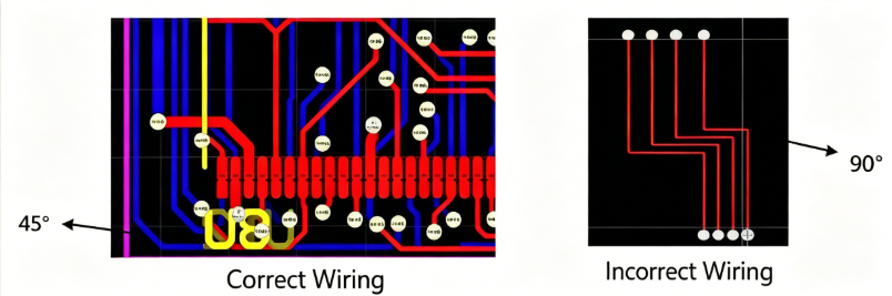
- Avoid acute and right-angle routes in PCB design, as they generate unnecessary radiation and result in poor PCB manufacturing processability.
- No vias shall be present on SMT pads to prevent solder paste loss and component cold solder joints. Important signal traces shall not pass through pin gaps.
PCB Routing for High-Frequency Circuits
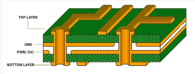
- Select the number of PCB layers rationally. The internal power layer (VCC layer) and ground layer (GND layer) provide shielding, effectively reducing parasitic inductance and parasitic capacitance, greatly shortening routing length, and minimizing crosstalk between signals.
- Routing method: Use 45° corners exclusively; do not use 90° corners.
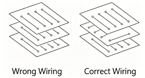
- Interlayer routing direction: Route perpendicularly between layers. If the top layer is horizontal, the bottom layer shall be vertical to reduce interference between signals.
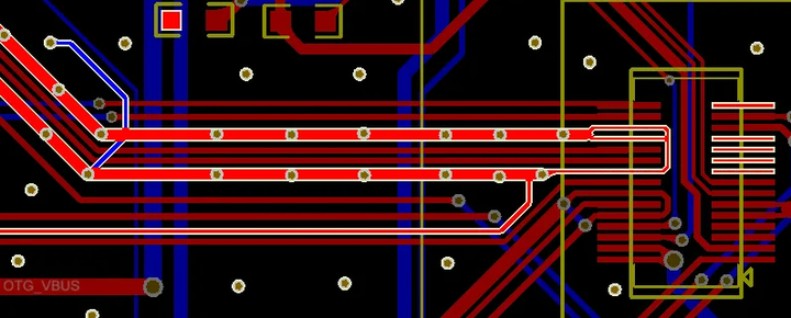
- Ground shielding: Apply ground shielding to important signals to significantly improve their anti-interference capability. Ground shielding can also be applied to interfering signals to prevent them from disturbing other signals.
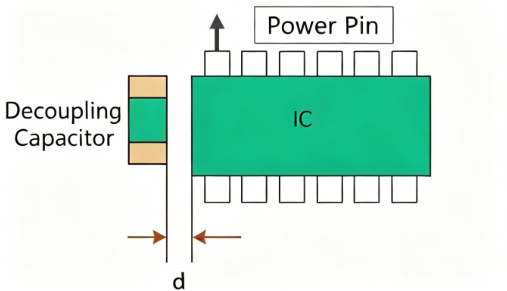
- Add decoupling capacitors: Install decoupling capacitors at the power pins of ICs.
- High-frequency choking: When a common ground exists between digital ground and analog ground, add high-frequency choking components between them, typically high-frequency ferrite beads with wires passing through their central holes.
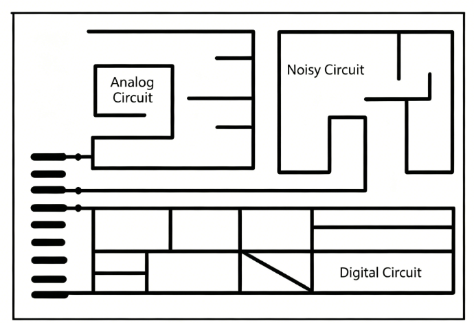
- Copper pouring: Increasing the grounded area reduces signal interference. (Remove dead copper during copper pouring.)
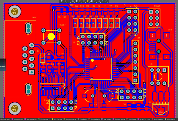
- Trace length: Shorter traces reduce interference. However, not all traces prioritize short length—for example, DDR routing requires equal length for clock, address, and data traces, so serpentine routing is often used to intentionally increase trace length.
Routing for Special Components
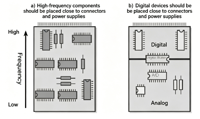
- High-frequency components: Keep connections between high-frequency components as short as possible to minimize distributed parameters and electrical interference. Components prone to interference shall not be placed close to each other.
a. Place high-frequency components near connectors and power sources.
b. Place digital devices near connectors.
- Components with high potential difference: Increase the distance between components and traces with high potential difference to avoid accidental short circuits and component damage. To prevent creepage, the distance between copper traces with a 2000V potential difference shall be greater than 2mm.
- Heavy components: Heavy components shall be fixed with brackets.
- Heat-generating and heat-sensitive components: Keep heat-generating components away from heat-sensitive components. Distribute high-power devices evenly.
Key Parameters for PCB Routing Design
- Copper trace (Track) width: 0.3mm for single-sided PCBs, 0.2mm for double-sided PCBs.
- Minimum clearance between copper traces: 0.3mm for single-sided PCBs, 0.2mm for double-sided PCBs.
- Minimum distance from copper traces to PCB edge: 1mm; minimum distance from components to PCB edge: 5mm; minimum distance from pads to PCB edge: 4mm.
- The pad diameter for standard through-hole components is twice the inner diameter of the pad.
- Electrolytic capacitors shall not be placed near heat-generating components such as high-power resistors, transformers, high-power transistors, three-terminal voltage regulators, and heat sinks. The distance between electrolytic capacitors and these components shall be no less than 10mm.
- No copper traces (except ground traces) or components shall be placed within 5mm of the radius of screw holes.
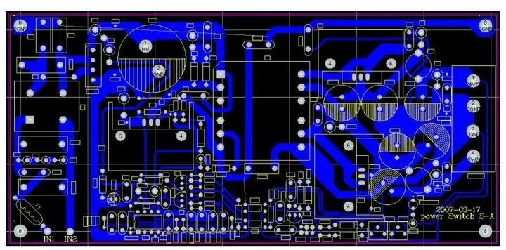
- For large-area PCB designs (over 500 square centimeters), leave a 5mm to 10mm wide component-free gap in the middle of the PCB to accommodate anti-warping pressure bars during wave soldering.
- Mark the wave soldering direction on each PCB with a hollow arrow.
- When routing, place DIP-packaged ICs perpendicular to the wave soldering direction and avoid parallel placement to prevent solder bridging.
- When routing transitions from vertical to horizontal, use a 45° transition.
- Power trace width: no less than 18mil; signal trace width: no less than 12mil; CPU I/O traces: no less than 10mil (or 8mil); trace spacing: no less than 10mil.
- Maintain uniform routing density across the board. Fill large density variations with mesh copper pouring, with a grid size greater than 8mil (or 0.2mm).
- No routing is allowed within the area ≤1mm from the PCB edge or within 1mm of mounting holes.
- Print warning marks on the silk screen layer near components such as fuses, fuse resistors, AC 220V filter capacitors, and transformers.
- The spacing between live and neutral wires in the AC 220V power section shall be no less than 3mm. The distance between any wire in the 220V circuit and low-voltage components, pads, and traces shall be no less than 6mm, with high-voltage markings printed on the silk screen. Separate strong current and weak current with thick silk screen lines to warn maintenance personnel.
About Maxipcb
Maxipcb empowers innovators to turn cutting-edge technologies into reality.
We offer one-stop solutions for design, simulation, testing, PCB manufacturing, component procurement and SMT assembly, enabling efficient development, rapid deployment and risk control across the full product lifecycle.Serving the world in communications, industrial automation, aerospace, automotive, semiconductor and beyond, we build a safer, more connected future together.
