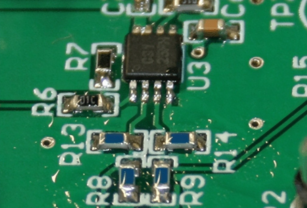
This article covers PCB soldering issues, wave soldering defects and corresponding preventive measures.
This article covers PCB soldering issues, wave soldering defects and corresponding preventive measures.
The following 13 types of wave soldering defects and preventive measures are mainly introduced:
- Blowholes and Pinholes
- Ball Joints/Excessive Fillets
- Cracked Joints
- Tombstoning
- Solder Residue
- Webbing and Solder Spattering
- Incomplete Joints
- Inconsistent or Poor Hole Filling
- Joint Contamination
- Pad Lifting
- Resist Peeling on PCB
- Pad Contamination
- Cold Joint (Insufficient Temperature)
1. What is Wave Soldering?
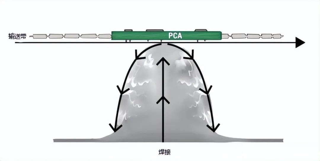
The basic principle of wave soldering is quite simple. After components are placed on the PCB and their leads are inserted into the drilled or punched holes ("through-holes") on the PCB, the assembly is placed on a conveyor belt. The conveyor belt moves the assembly through a tank of molten solder (commonly referred to as a "pot"). Solder is pumped through a chimney to form a ridge that flows over the bottom of the PCB, creating connections between component leads and PCB circuits.
Although the principle is simple, the process requires control of many variables, each of which can lead to serious defects.
Wave soldering has been applied to solder surface mount devices ("SMD"), but the technology is most suitable for "through-hole" components (components with leads inserted into drilled holes of the circuit board).
2. Wave Soldering Process
When designing a PCB for wave soldering, PCB Layout engineers need to pay attention to 3 issues:
- Pad Spacing: If pads to be soldered are too close, molten solder will flow between them, resulting in short circuits not only between the two connected pads but also potentially the entire PCB.
- Solder Mask: A layer of solder mask is usually applied on the PCB. However, careful inspection of the solder mask is necessary to prevent unnecessary errors.
- Flux: Once the pad spacing and solder mask of the PCB to be soldered are checked, flux is required. Flux helps ensure that the PCB areas to be soldered are clean and free of oxidation.
3. Wave Soldering Defects and Preventive Measures
1. Blowholes and Pinholes
(1) Pinholes and Blowholes
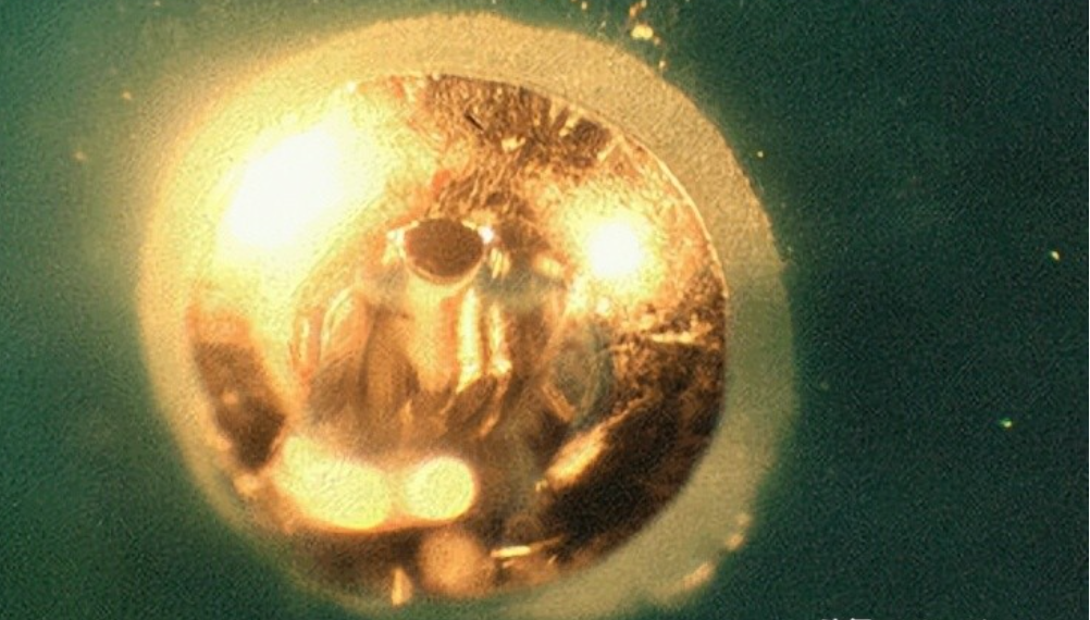
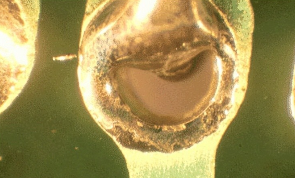
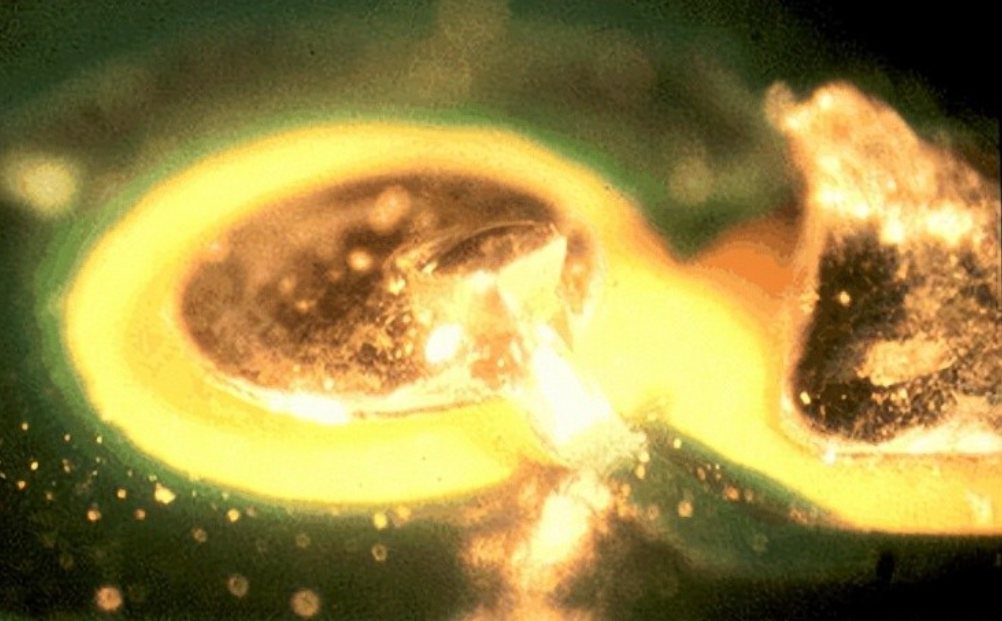
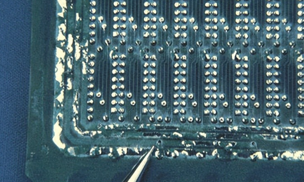
Pinholes or blowholes are mainly caused by outgassing of the printed circuit board during the soldering process. The formation of pinholes and blowholes during wave soldering is usually related to the thickness of copper plating.
During the soldering operation, moisture inside the circuit board is heated into gas, which escapes through the solder while it is still molten. When the gas continues to escape as the solder joint solidifies, voids are formed. The circuit may conduct temporarily, but long-term poor conduction is likely to occur.
(2) Causes
- Insufficient top temperature of the PCB
- Excessive moisture accumulated in the circuit board attempts to escape through the thin copper plating layer.
- Similar types of components are not oriented in the same direction, resulting in poor copper plating.
- The lead-to-hole ratio is either too small or too large.
(3) Solutions
- Improve circuit board quality by plating at least 25μm of copper in the through-holes.
- Baking is commonly used to eliminate outgassing by drying the board; however, baking removes moisture from the board but does not address the root cause.
(4) Preventive Measures
- Verify the top PCB temperature, verify flux deposition and required preheating temperature, check for moisture in the laminate and perform pre-baking if necessary, and inspect through-hole plating.
2. Ball Joints/Excessive Fillets
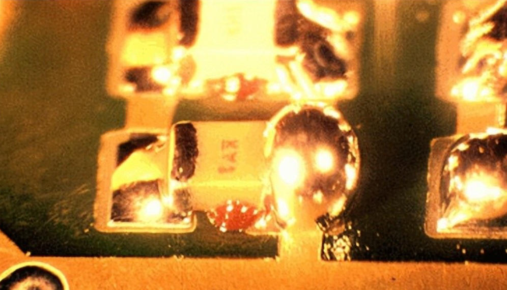
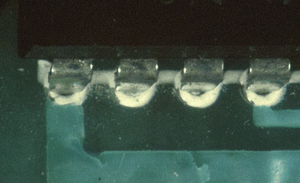
A solder joint on a chip component that exceeds the height of the component with a convex meniscus is defined as a ball joint or excessive fillet. It occurs during the separation of the board from the solder wave and is more common in nitrogen soldering.
3. Cracked Joints
Solder joint cracking on plated through-hole joints is uncommon.
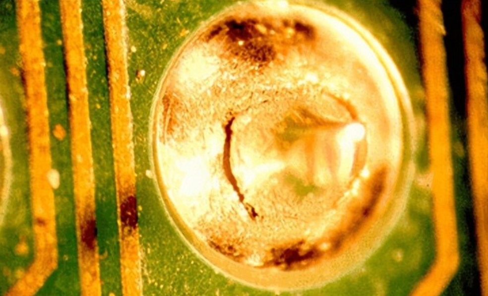
(1) In the figure below, the solder joint is on a single-sided board, and the joint has failed due to the expansion and contraction of the lead in the joint.
In this case, the failure lies in the initial design, as the circuit board does not meet the requirements of its operating environment. Single-sided joints may fail during assembly due to improper handling, in which case the joint surface will show stress lines generated during repeated movement.
The stress lines here indicate that this crack on the single-sided board is caused by repeated movement during processing.
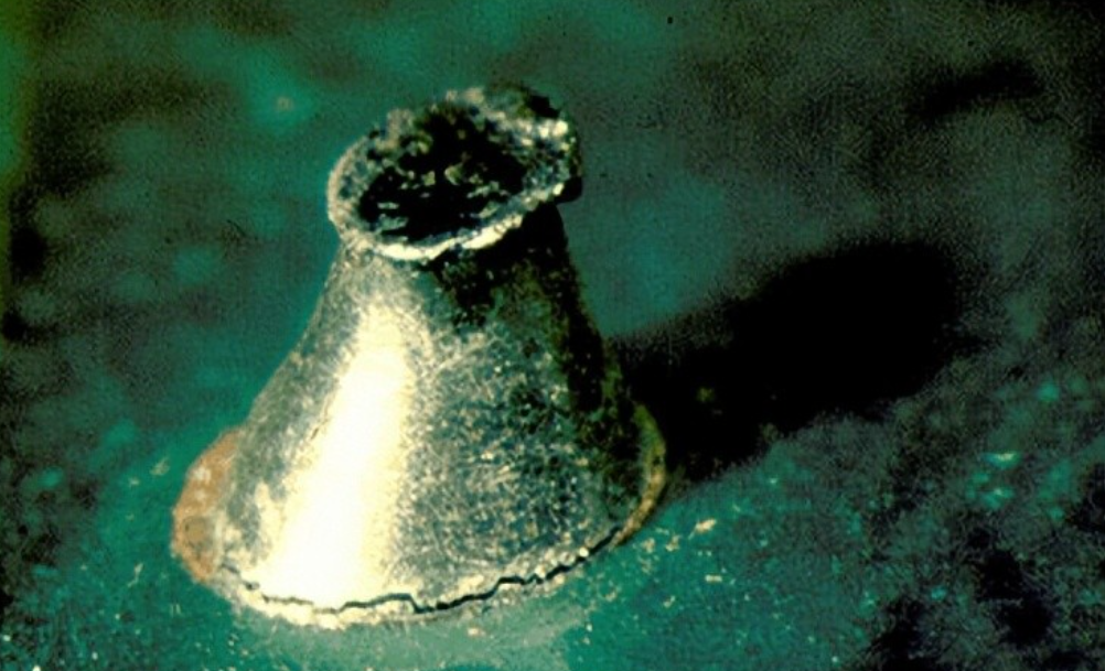
(2) The figure below shows cracks around the bottom of the fillet, separated from the copper pad, which is most likely related to the basic solderability of the circuit board.
No wetting occurs between the solder and the pad surface, leading to joint failure. Joint cracking usually occurs due to thermal expansion of the joint, which is related to the original product design.
4. Tombstoning
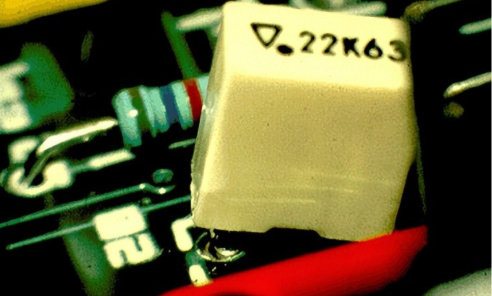
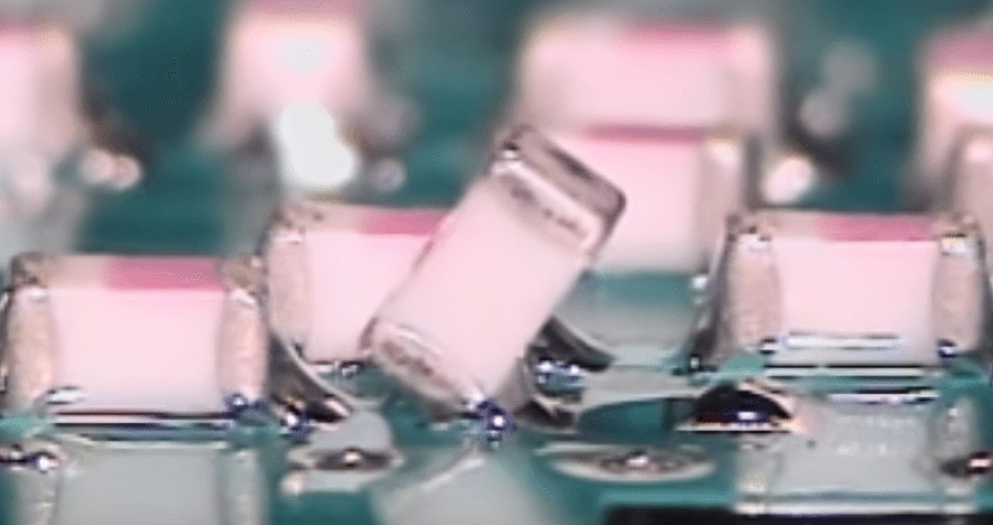
Lifted components, also known as tombstoning, are components lifted from the board during the soldering process.
(1) In the case shown in the figure below, the component is lifted due to thermal demand on the leads. This issue can be resolved simply by increasing the immersion time in the solder wave.
Causes of component lifting:
- Incorrect lead length causes leads to hit the solder pot and lift during wave entry.
- Board bending, common in large connectors, IC sockets or large IC packages; essentially, the board bends while the components remain stationary.
- Turbulent waves for surface mount applications lift lightweight components.
- Components with different thermal demands or lead solderability may also lift during wave contact.
- Unrelated to the solder wave, vacuum-formed shrink wrap may cause lifting during wave contact.
Shrink wrap is sometimes used to secure components to the circuit board surface for lead cutting; it can be pulled under leads, causing components to lift during wave contact.
(2) In the case shown in the figure below, the component was not properly inserted before entering the soldering process.
(3) Solutions
- To fix incorrect lead length: Check the leads used; long leads hitting the solder pot will be pushed out of the holes. Increase immersion time in the solder wave to reduce thermal demand on leads and stabilize them.
- To correct PCB bending or other bending-related issues: Carefully inspect the PCB type and its heat capacity difference. Board bending is common on large connectors, large IC packages or sockets. PCBs that are bent from the start (e.g., plastic) should not undergo wave soldering, as wave soldering will cause the plastic to bend and lift components off the board.
- Finally, check the heat capacity difference of the circuit board and all components. Components with different temperature requirements or lead solderability temperatures will also lift during wave contact, as some components solder down while excessive heat pushes others away.
5. Solder Residue
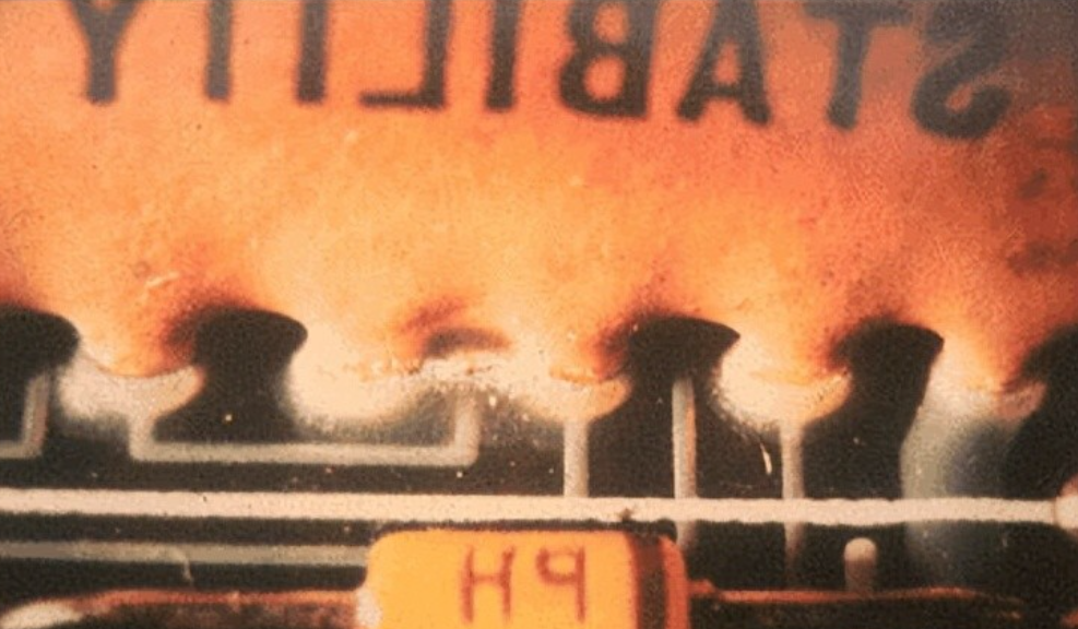
Visible flux residue on boards is more common due to reduced use of cleaning agents in the industry.
In the figure below, the residue results from either the flux formulation or poor process conditions. Many no-clean materials rely on correct preheating temperatures to minimize residue left on the board.
Wave contact time may also affect residue left on the board; discussions with flux suppliers should provide correct process parameters.
The flux residue here may be caused by the flux formulation or poor process conditions.
6. Webbing and Solder Spattering
(1) Webbing and Solder Spattering
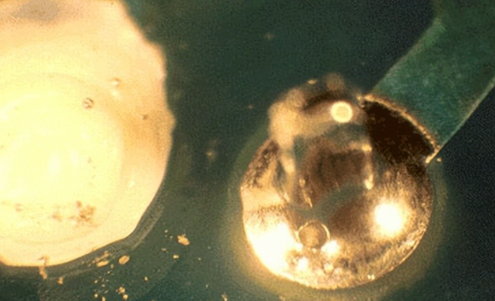
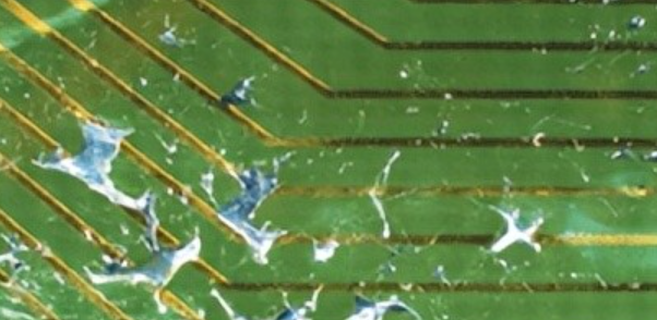
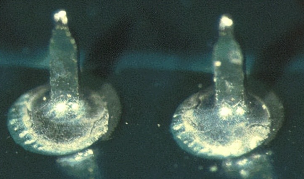
As shown in the two figures below: these solder flakes adhere to the solder mask in messy splatters, presenting a spiderweb-like appearance.
(2) Causes
- Insufficient flux usage or contaminants on the board surface during wave soldering.
- Unstable soldering iron temperature also causes this issue; solder spattering/webbing may lead to short circuits.
(3) Solutions
- Easily removed with a knife tip or tweezers.
(4) Preventive Measures
- If excessive rosin-based flux in solder wire is the cause, reduce the amount of solder wire additives.
- If unstable soldering iron temperature is the cause, use a constant-temperature soldering station.
- Keep the board surface clean.
7. Incomplete Joints
Incomplete solder fillets are often seen on single-sided boards after wave soldering.
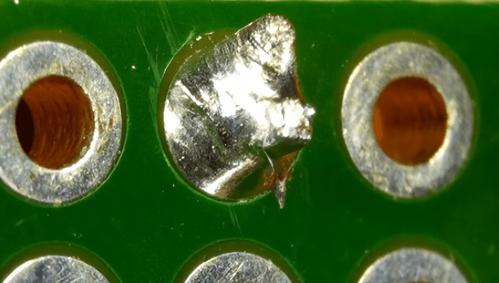
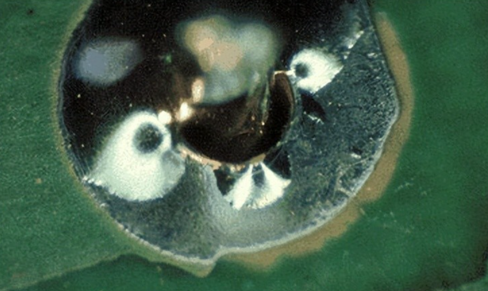
(1) In the figure below, an excessive lead-to-hole ratio causes soldering difficulties. The pad edges also show signs of resin smearing.
The example shown in the figure results from burrs on the copper pad. During drilling or punching, copper on the circuit board surface is deflected in some areas, leading to soldering difficulties. The same occurs if resin is smeared on pad edges.
(2) Causes
- Poor lead-to-hole ratio
- Steep conveyor angle
- Excessively high wave temperature
- Contamination on pad edges
(3) Preventive Measures
- Soldering performance may be improved by reducing the conveyor angle from 6° to 4°. This reduces the wave's drainage performance but may cause short circuits.
- Lower the wave temperature.
- The lead-to-hole ratio is typically the lead diameter plus 0.010".
8. Inconsistent or Poor Hole Filling
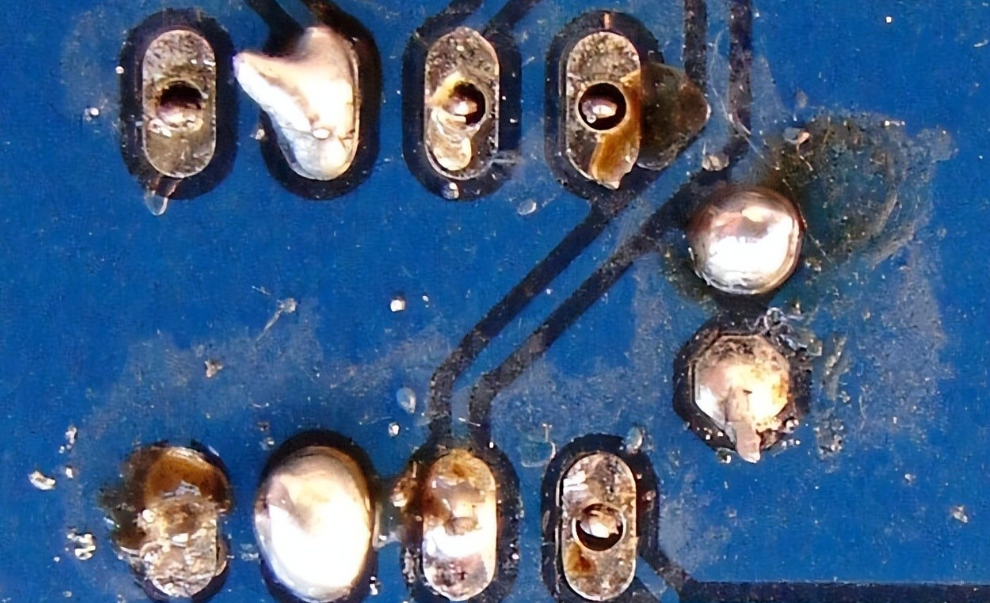
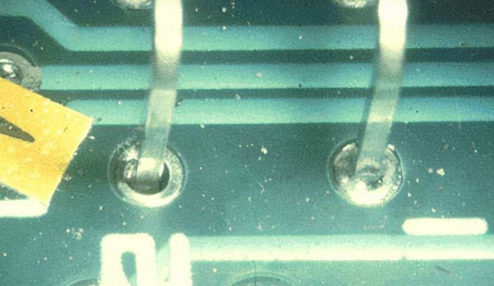
(1) Solder does not completely fill the plated through-holes shown in the figure below. This is caused by insufficient preheating settings or poor flux application. In both cases, reviewing process parameters should resolve the issue.
This is a common problem when switching from foam flux to spray flux units, as flux struggles to penetrate through-holes.
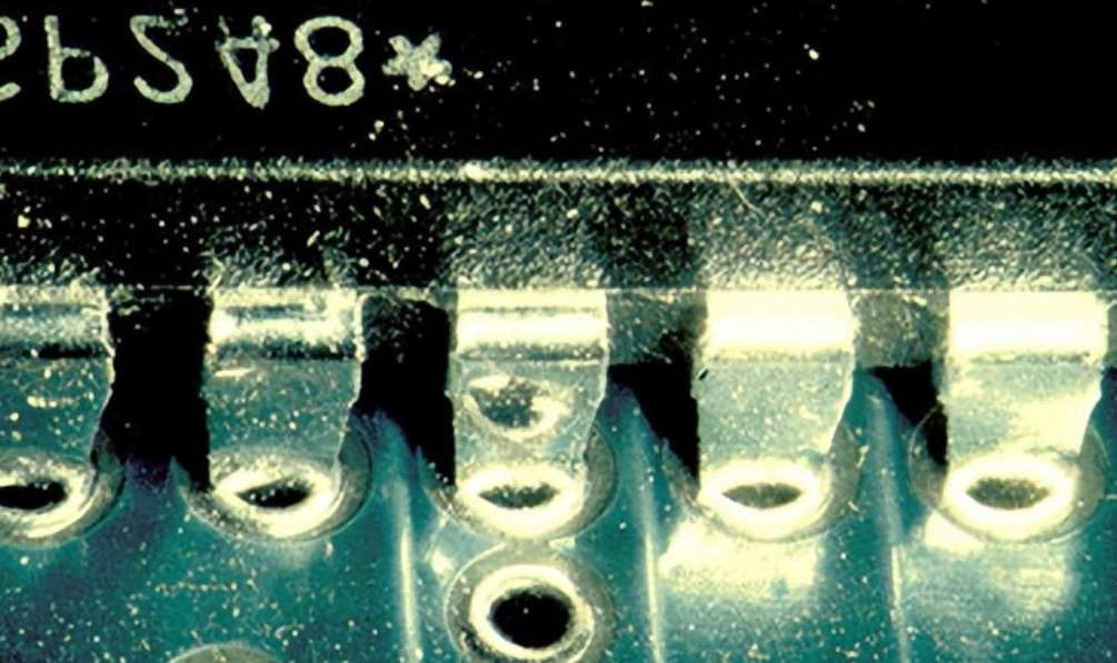
(2) In the figure below, poor hole filling is caused by preheating settings. Solder wets the component leads but fails to wet the through-hole surfaces.
The top temperature of the printed board before wave contact should be 100–110°C, typically applicable to double-sided and multilayer boards. Single-sided boards are processed at slightly lower temperatures as solder penetration is not required.
(3) Solder does not completely fill the plated through-holes shown in the figure below. This may be caused by insufficient preheating settings or poor flux application. In both cases, reviewing process parameters should resolve the issue.
Solder does not completely fill the plated through-holes on the left side.
(4) In the figure below, one hole is filled and the second is not, indicating the issue is unlikely related to the printed board. This occurs because the solder solidifies on one hole due to the component's thermal demand. This can be easily resolved by increasing preheating or extending wave contact time.
(5) In the figure below, there is no sign of solder in the through-holes. The board most likely failed to contact the solder wave due to insufficient wave height, finger damage, or poorly maintained pallets. Incorrectly loading the circuit board into the system may also cause this failure.
Poor through-hole plating quality may be a factor, but this is unlikely.
(6) The example of poor hole filling in the figure below is unique, as the issue is caused by legends on the printed board. Careful inspection reveals that poor design rules caused legends to contaminate the tops of plated through-holes. Solder fails to rise in the holes or wet the pad surfaces. In this case, the legends provide no benefit, and new design rules must be applied.
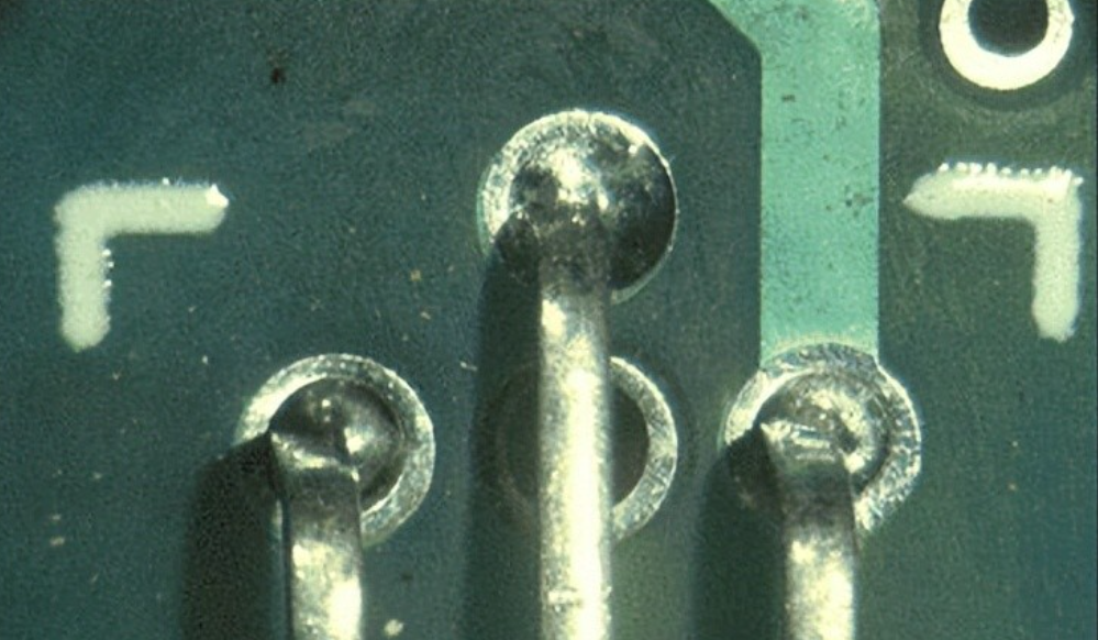
(7) The figure below shows poor wettability on the pad surface, likely due to the thickness of the tin/lead coating. Solder leveling typically leaves a thin deposit on the pad surface and hole edges. This defect is commonly called the "weak knee effect", where solder fails to wet the knee of the hole and the pad.
Poor hole filling may also be caused by insufficient preheating settings or poor flux application.
Preventive Measures:
- Verify flux deposition, verify preheating temperature, check wave height, check lead-to-hole aspect ratio, verify internal ground planes.
9. Joint Contamination
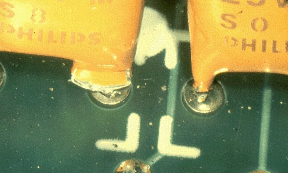
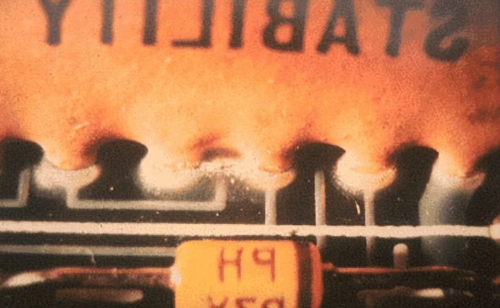
The tops of the plated through-holes in the figure below were contaminated during the soldering operation. High temperatures softened the coating on the resistor network and contaminated the circuit board surface.
The top board temperature is typically 100–110°C during preheating and may exceed 190°C when contacting the solder wave. The component should not cause this issue under normal process conditions; the compatibility of the component with the soldering process should be re-evaluated.
10. Pad Lifting
Pad lifting is rarely seen on plated through-hole boards but may occur on single-sided boards during assembly.
(1) The issue shown in the figure below occurs directly when handling components after wave soldering. The adhesion of copper foil decreases as surface temperature rises, so copper foil adhesion is very low after soldering. Any handling or force applied to the component may cause pad lifting.
Care is required when lifting the board from the conveyor or pallet, as operators often use large components as handles.
This pad lifting occurred during handling after wave soldering.
Causes of pad lifting may include:
- Excessive processing of pad joints where the layer between copper and the circuit board is damaged.
- Circuit boards designed with thin copper layers.
- Lack of uniform copper plating on leads of through-hole components.
(2) Solutions
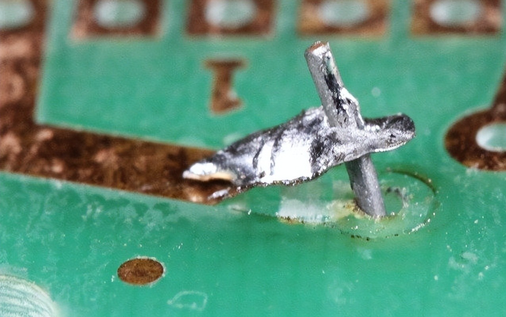
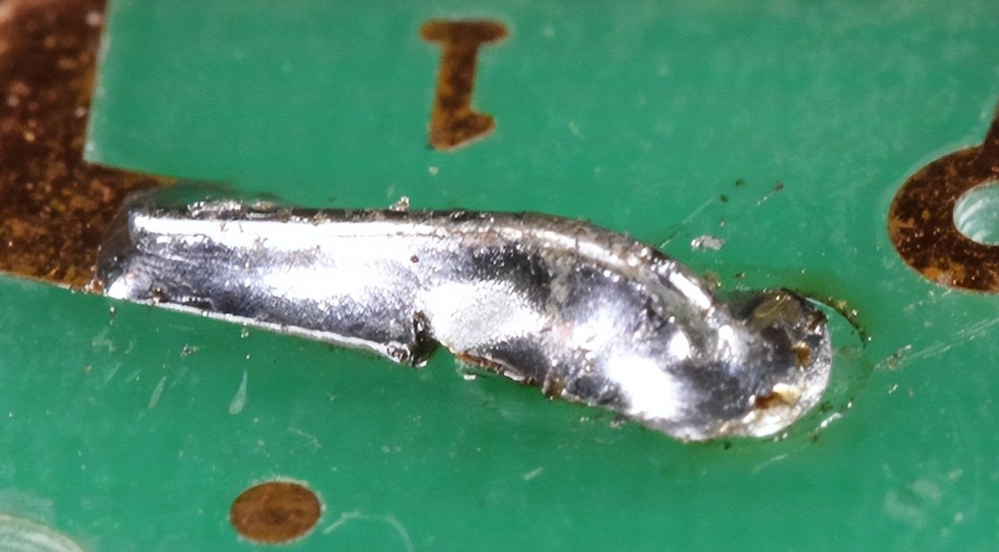
- The simplest fix is to fold the lead onto the still-connected copper trace and solder it, as shown in the figure below. If solder mask is present, it must be carefully scraped off to expose bare copper.
- Other alternatives: Follow the trace to the next through-hole and run a jumper wire there.
- Or, in the worst case: Follow the trace to the nearest component and solder a jumper wire to the component's pins.
11. Resist Peeling on PCB
The figure below shows a clear example of resist peeling from the circuit board surface after soldering. Simply put, this is caused by incorrect specifications of the printed circuit board.
Tin/lead should not be used as resist on professional circuit boards. When tin/lead melts, it expands and may cause loss of adhesion between solder and resist.
If the resist is brittle or thin, it will separate as shown in the figure below. Tin/lead may be used if the coating thickness is less than 3–5μm, as minimal movement occurs during wave soldering or reflow soldering.
12. Pad Contamination
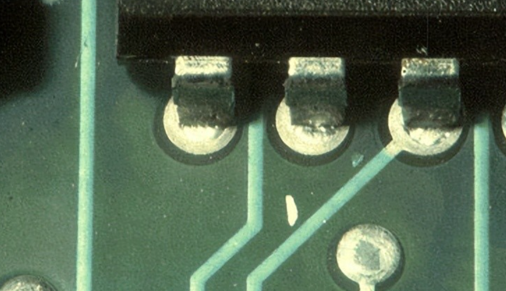
(1) The solder joint shown in the figure below is acceptable, but solder mask on the pad reduces the solder volume. Resist on the board is directly related to poor design rules used on this printed board.
The correct design rule for resist apertures is a 0.002–0.003" annular ring around the pad.
The example in the figure is designed with a resist aperture smaller than the pad size. It is worth noting that solder mask on pads may affect joint appearance during wave soldering but does not cause reliability issues.
(2) Solutions
- Use reduced resist apertures to eliminate solder shorts.
- If design changes are not desired, use glue dots. Placing an additional glue dot between consistently shorted leads is a simple fix.
13. Cold Joint
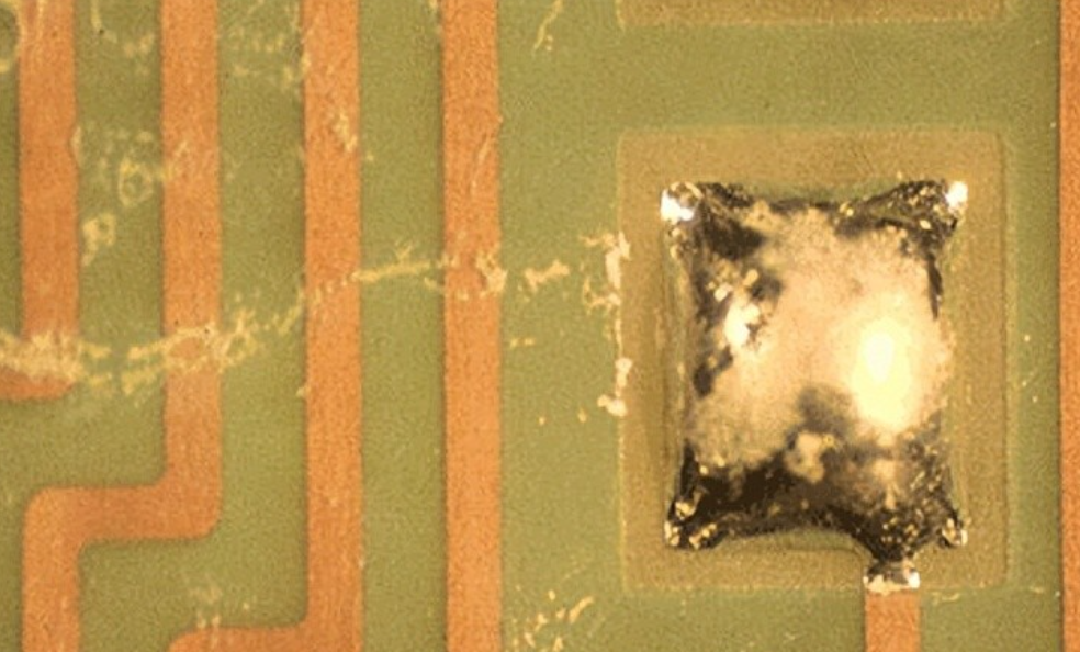
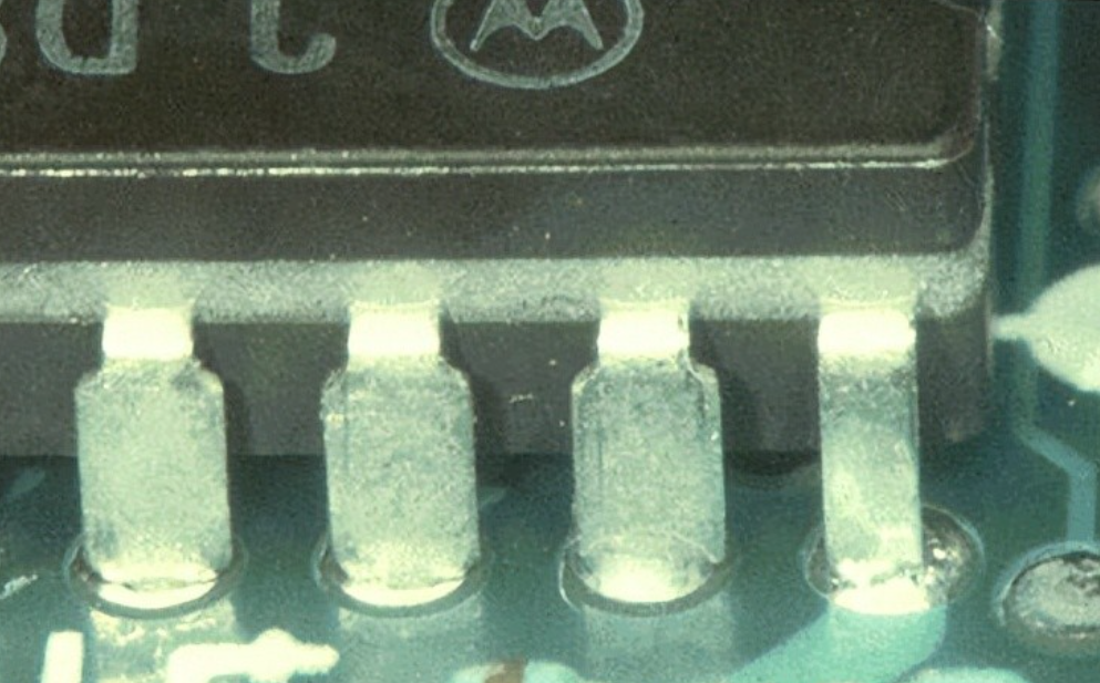
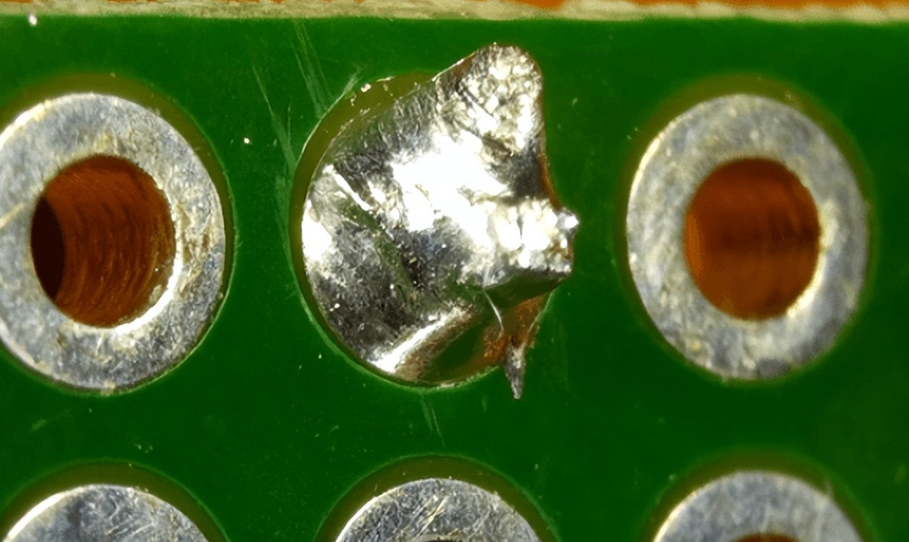
(1) The figure below shows a lumpy, dull cold joint. The surface of a cold joint appears dull, uneven and pitted.
A cold joint is equivalent to a dry joint, which is difficult to fully detect during production and often emerges after the user has used the product for days, months or even years. It not only produces extremely adverse effects but also causes serious consequences, as cold joints have low strength and poor electrical conductivity.
(2) Causes
- Insufficient heat transferred to the joint to achieve complete melting.
- The soldering iron or joint itself may not have sufficient time to fully heat up.
- The soldering iron temperature may not be set high enough to melt the specific solder type used (e.g., lead-free solder has a higher melting temperature), or this may result from the design of the pads and traces themselves.
- A pad directly connected to a ground plane without considering heat dissipation causes heat from the soldering iron to dissipate into the ground plane.
(3) Solutions
- To repair a cold joint, simply reheat the joint with a hot soldering iron until the solder flows.
 About Maxipcb
Maxipcb empowers innovators to turn cutting-edge technologies into reality.
We offer one-stop solutions for design, simulation, testing, PCB manufacturing, component procurement and SMT assembly, enabling efficient development, rapid deployment and risk control across the full product lifecycle.Serving the world in communications, industrial automation, aerospace, automotive, semiconductor and beyond, we build a safer, more connected future together.