The PCB design process consists of a series of industrial design steps, which is a key link to ensure the quality of mass-produced circuit board products and reduce troubleshooting.
The PCB design process consists of a series of industrial design steps, which is a key link to ensure the quality of mass-produced circuit board products and reduce troubleshooting. PCB is the foundation of industrial electronic product design. Whether it is small-batch production or large-scale production of consumer electronics, PCB design is included in almost all design technologies. Due to the complexity of the design process, many common mistakes occur repeatedly. The following lists the five most common design problems in PCB design and corresponding countermeasures.
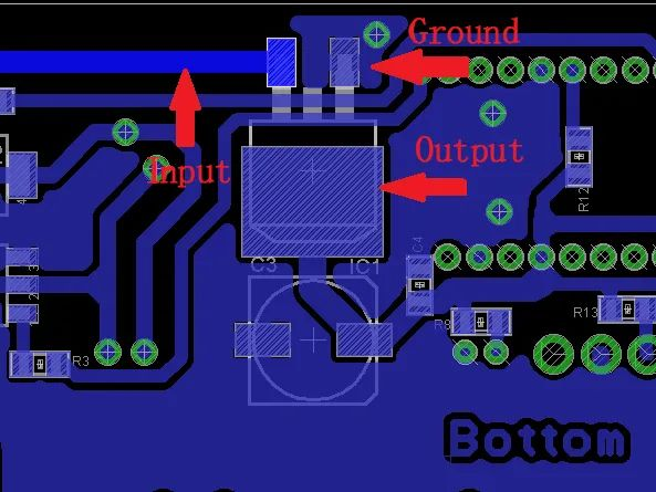
01 Pin Errors
Series linear regulated power supplies are cheaper than switching power supplies, but have lower energy conversion efficiency. Usually, many engineers choose linear regulated power supplies due to their ease of use and low cost. However, it should be noted that although they are convenient to use, they consume a lot of electrical energy and cause a large amount of heat dissipation. In contrast, switching power supplies are more complex to design but have higher efficiency. However, it should be noted that the output pins of some regulated power supplies may be incompatible with each other, so it is necessary to confirm the relevant pin definitions in the chip datasheet before routing.
02 Routing Errors
The difference between design and routing is the main cause of errors in the final stage of PCB design. Therefore, it is necessary to repeatedly check things such as device dimensions, via quality, pad sizes, and review levels. In short, it is necessary to repeatedly confirm and check against the design schematic.
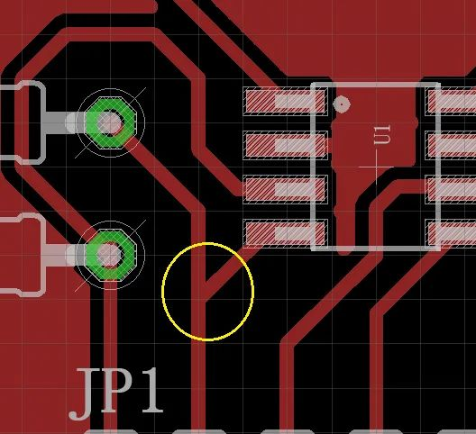
03 Acid Traps
When the included angle between PCB leads is too small (presenting an acute angle), an acid trap may be formed. These acute-angle connections may retain etching solution during the circuit board etching stage, thereby removing more copper at that location and forming stuck points or traps. This may cause lead breakage and open circuits in the later stage. This phenomenon of acid traps has been greatly reduced in modern manufacturing processes due to the use of photosensitive etching solutions.
04 Tombstoning
When soldering small surface-mount devices using the reflow process, the devices may form a single-end lifting phenomenon under the infiltration of solder, commonly known as "tombstoning". This phenomenon is usually caused by an asymmetric routing pattern, which results in uneven heat dissipation on the device pads.
05 Lead Width
When the current of a PCB lead exceeds 500mA, the conventional wire diameter will be insufficient. For the same thickness and width, the conductors on the PCB surface can pass more current than the internal conductors of a multilayer circuit board, because the surface leads can dissipate heat through air flow. The line width is also related to the copper foil thickness of the layer where it is located. Most PCB manufacturers allow you to choose copper foil thicknesses ranging from 0.5 oz/sq.ft to 2.5 oz/sq.ft.