Definition of PCB Layers
Solder Mask
The solder mask layer defines areas where solder resist (commonly known as green oil) is excluded from the PCB. Since this layer adopts negative output, areas with solder mask patterns will not be covered by green oil during production; instead, they will be plated with tin and appear silvery white.
Paste Mask
The paste mask layer is dedicated to surface mounting processes and corresponds to all pads of SMT components. It shares the same outline size as the top layer and bottom layer. This layer is used to fabricate stencils for solder paste dispensing during assembly.
Key Notes
Both layers are designed for soldering purposes, which means neither of them is exclusively for green oil coating. Many people wonder: is there an independent layer that represents green oil coverage (i.e. areas marked with this layer will be fully coated with insulating green oil)? So far, no such independent layer has been found.
By default, all pads on a designed PCB are assigned with solder mask patterns. Therefore, the finished PCB has silvery tin plating on pads without green oil coverage, which is a normal phenomenon. In contrast, PCB traces are only drawn on the top layer or bottom layer with no solder mask patterns attached, yet all traces on the manufactured PCB are fully covered with green oil.
The working principles can be summarized as follows:
- The solder mask layer creates openings on the overall green oil coating to expose copper for soldering.
- All areas without solder mask patterns will be covered with green oil by default.
- The paste mask layer is specially used for SMT packages.
- An SMT device layout involves the Top Layer, Top Solder and Top Paste. The Top Paste has the same size as the Top Layer, while the Top Solder is slightly larger than the two.
- A through-hole (DIP) device layout only requires the Top Solder and Multi-Layer. After analysis, the Multi-Layer is essentially the overlapping area of the Top Layer, Bottom Layer, Top Solder and Bottom Solder. Similarly, the Top Solder and Bottom Solder are slightly larger than the Top Layer and Bottom Layer respectively.
Related Question
Is the statement "Only copper areas with corresponding copper foil can be tinned or gold-plated where solder mask patterns are placed" correct? This view was put forward by a PCB factory technician. Its meaning is: to achieve tin plating on areas defined by solder mask patterns, there must be corresponding copper foil (i.e. matching patterns on the Top Layer or Bottom Layer) beneath the solder mask.
Conclusion: This statement is correct. The solder mask layer marks areas that are not covered by green oil.
Common PCB Layer Definitions
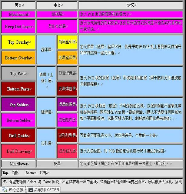
- Mechanical Layer: Defines the overall outline and physical dimension of the entire PCB.
- Keep-out Layer: Sets the boundary for electrical routing. Traces with electrical characteristics cannot extend beyond the scope defined by this layer.
- Top Overlay: Top silkscreen layer for printing component designators and text markings on the PCB top side.
- Bottom Overlay: Bottom silkscreen layer for printing text and symbols on the PCB bottom side.
- Top Paste: Top pad layer for SMT solder paste application.
- Bottom Paste: Bottom pad layer for SMT solder paste application.
- Top Solder: Top solder mask layer.
- Bottom Solder: Bottom solder mask layer.
- Drill Guide: Drill reference layer.
- Drill Drawing: Drill plot layer.
- Multi-Layer: A virtual layer covering all physical layers of the PCB.
Detailed Explanation
The mechanical layer is used to define the overall profile of the PCB. The keep-out layer restricts the routing area for conductive traces. The top and bottom overlay layers carry printed information such as component reference numbers and labels visible on finished boards.
For the top paste and bottom paste layers: They correspond to exposed copper pads. For example, a trace drawn on the top layer will be fully covered by green oil in mass production. If you draw a square or dot pattern on the top paste layer at the same position, the corresponding area on the finished PCB will have no green oil, exposing the raw copper.
The top solder and bottom solder work oppositely to the paste layers. Again, due to negative output characteristics, areas with solder mask patterns are opened for tin plating, while the rest are covered with green oil.
The multi-layer is a virtual layer equivalent to the mechanical layer in nature, representing all layers of the PCB. Pads and through-holes must be assigned to the multi-layer; otherwise, they will not be displayed normally.
9 Major PCB Layer Categories (Protel 99 SE)
1. Signal Layer
Signal layers are mainly used for laying out conductive traces on PCBs. Protel 99 SE provides 32 signal layers in total, including one Top Layer, one Bottom Layer and 30 Mid Layers.
2. Internal Plane Layer (Power/Ground Plane)
Protel 99 SE supports 16 internal power/ground planes. This type of layer is exclusively used for multi-layer PCBs to route power lines and ground lines. The specifications of double-layer, four-layer and six-layer PCBs are generally defined by the number of signal layers and internal power/ground planes.
3. Mechanical Layer
Protel 99 SE offers 16 mechanical layers. They are applied to define PCB outline dimensions, datum marks, alignment marks, assembly notes and other mechanical information, which vary according to the requirements of design institutes and PCB manufacturers. You can add more mechanical layers via the menu command: Design | Mechanical Layer. Mechanical layers can also be combined with other layers for output and display.
4. Solder Mask Layer
A layer of solder resist coating is applied to all areas except pads to prevent unintended tin adhesion. The solder mask layers are automatically generated to match pad layouts during design. Protel 99 SE provides two solder mask layers: Top Solder and Bottom Solder.
5. Paste Mask Layer (SMD Stencil Layer)
It shares similar functions with the solder mask layer, but is tailored for pads of surface-mount devices during automated soldering. Protel 99 SE is equipped with Top Paste and Bottom Paste layers.
This layer is dedicated to SMT components. If the PCB is fully populated with through-hole (DIP) components, there is no need to export Gerber files for this layer. Solder paste must be applied to every SMT pad before component mounting, and the paste mask Gerber file is essential for manufacturing the corresponding stencil and production film.
It is critical to distinguish between the paste mask and solder mask layers. Their film outputs look similar, yet they serve completely different purposes.
6. Keep-out Layer
This layer defines valid areas for component placement and trace routing on the PCB. Draw a closed boundary on this layer to mark the working area; automatic component placement and routing will not be executed outside this boundary.
7. Silkscreen Layer
Silkscreen layers are used to print graphical and text information, including component outlines, reference designators and annotations. Protel 99 SE provides Top Overlay and Bottom Overlay. In most cases, all text labels are placed on the top silkscreen layer, and the bottom silkscreen layer can be disabled.
8. Multi-Layer
Pads and through-vias run through the entire PCB to form electrical connections between different conductive layers, hence the virtual multi-layer is specially designed for this purpose. Pads and vias must be assigned to the multi-layer, otherwise they cannot be displayed normally.
9. Drill Layer
Drill layers provide drilling information for PCB fabrication (drilling is required for pads and vias). Protel 99 SE includes two drill layers: Drill Guide and Drill Drawing.
Distinction Between Solder Mask and Paste Mask
- Solder Mask: This layer defines green oil exclusion areas. With negative output, areas marked with solder mask patterns are opened for tin plating and present a silvery appearance without green oil coverage.
- Paste Mask: Used for automated SMT assembly, matching all SMT pad positions. It has the same size as the top/bottom copper layers and is used to produce stencils for solder paste printing.
Key Recap
Both layers are related to soldering, rather than one for tinning and the other for green oil coating. There is no independent layer that solely represents green oil coverage.
On standard PCB designs, pads are assigned with solder mask patterns by default, so finished pads are tinned without green oil. Traces are only drawn on the top or bottom layer with no solder mask patterns, and thus are fully covered by green oil after production.
- The solder mask creates openings on the green oil coating for soldering.
- All areas without solder mask patterns are covered with green oil by default.
- Rules for different packages:
- SMT Package: Uses Top Layer, Top Solder and Top Paste. The Top Paste is identical in size to the Top Layer, while the Top Solder is slightly larger.
- DIP Package: Uses Top Solder and Multi-Layer. The Multi-Layer is the overlapping area of Top Layer, Bottom Layer, Top Solder and Bottom Solder. The Top/Bottom Solder is slightly larger than the corresponding Top/Bottom Layer.
