With the development of semiconductor integration, electronic products such as mobile phones, laptops and smart watches demand small size, portability, excellent electrical performance and low cost. Packaging technology is one of the key factors to improve performance and reduce cost. Package-on-Package (PoP) is an effective solution to chip packaging challenges for mobile devices.
1. What is Package-on-Package (PoP)
With the development of semiconductor integration, electronic products such as mobile phones, laptops and smart watches demand small size, portability, excellent electrical performance and low cost. Packaging technology is one of the key factors to improve performance and reduce cost. Package-on-Package (PoP) is an effective solution to chip packaging challenges for mobile devices.
PoP is formed by stacking two or more packages vertically, essentially a
3D stacking technology.
Soldering between PoP layers and between the bottom package and the PCB is achieved by
BGA solder balls, which provide electrical and thermal paths between layers.
Common configurations:
- Bottom package: Processor
- Top package: Memory
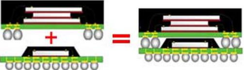
Figure 1 – A typical PoP structure
2. Solder Paste Pad Printing Process
To attach BGA solder balls to the PCB, PoP usually uses standard stencil printing to deposit small solder paste dots on the PCB, then mounts the bottom package solder balls onto these dots.
- BGA on PCB: Bottom BGA
- BGA connecting top and bottom packages: Top BGA
The top BGA surface cannot be printed with solder paste, so
pad printing is required.
In pad printing:
The top BGA solder balls dip directly into solder paste or flux, then are mounted onto the bottom BGA in one step. After both packages are placed, the assembly goes through reflow soldering.
PoP Assembly Flow
- Print solder paste
- Place bottom package
- Dip top package in flux / PoP paste
- Place top package
- Reflow
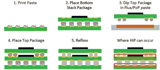
Figure 2 – PoP assembly flow chart
3. Key Notes for PoP Process
- The solder paste for PoP dipping has very low viscosity, about 50 Pa·s; standard printing paste is too viscous and not suitable.
- The dipping height of top BGA into solder paste / flux must be adjusted properly.
- The mounter must recognize BGAs after dipping.
- Top BGA placement requires high positional accuracy.
- Control placement pressure and height.
4. PoP Solder Paste
Maxipcb have solder pastes in
low‑temperature, medium‑temperature and high‑temperature series, suitable for different reflow profiles.
Advantages: stable viscosity, long stencil life, high mechanical strength after soldering.
About Maxipcb
Maxipcb empowers innovators to turn cutting-edge technologies into reality.
We offer one-stop solutions for design, simulation, testing, PCB manufacturing, component procurement and SMT assembly, enabling efficient development, rapid deployment and risk control across the full product lifecycle.Serving the world in communications, industrial automation, aerospace, automotive, semiconductor and beyond, we build a safer, more connected future together.
