The PCB is an indispensable part of electronic products, providing electrical and mechanical interconnection for the circuit system. Proper component arrangement is critical for stable and reliable performance, especially for integrated circuits. Poor layout degrades function or causes failure. This article introduces key considerations for RF PCB design.
1. Overview
The PCB is an indispensable part of electronic products, providing electrical and mechanical interconnection for the circuit system. Proper component arrangement is critical for stable and reliable performance, especially for integrated circuits. Poor layout degrades function or causes failure. This article introduces key considerations for RF PCB design.
2. Layout Guidelines
2.1 Mechanical Structure Requirements
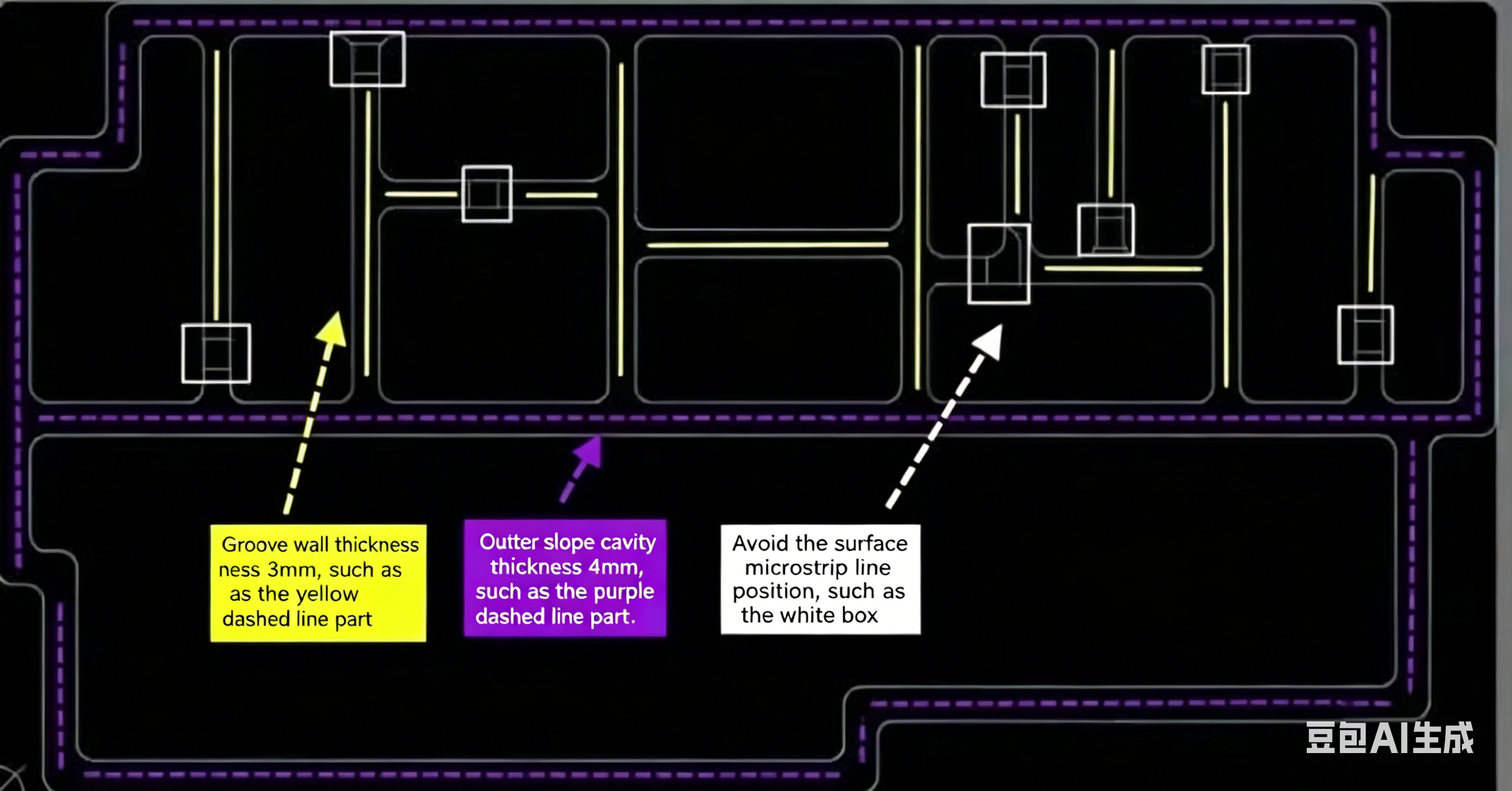
Clarify product structure before layout, including cavity dimensions, screw sizes, and corner radii.
- Typical outer cavity thickness: 4 mm
- Inner cavity width: 3 mm (2 mm for dispensing process)
- Corner radius: 2.5 mm
- Positioning: Use grid multiples of 0.5 mm (minimum 0.1 mm) for precision machining.
Structural outline drawing of finished PCB design
2.2 General Layout Rules
- Prioritize the RF signal chain layout, then other circuits.
- Follow the schematic sequence (input → output).
- Arrange components in straight line or L‑shape.
- Keep tight spacing for networks such as π‑networks.
Straight‑line RF chain layout example (left‑to‑right signal flow)
When space is limited, a U‑shape is acceptable but requires a middle cavity wall for shielding to avoid interference and self‑oscillation.
U‑shaped layout with isolation cavity
Add transverse isolation walls for:
- Sensitive circuits
- High‑gain paths (to prevent self‑oscillation)
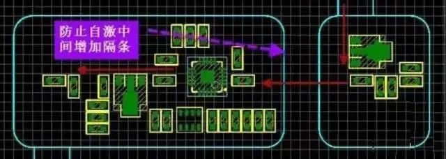
Straight layout with transverse isolation barrier for self‑oscillation prevention
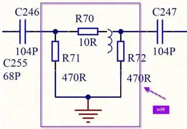
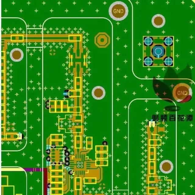
2.3 Peripheral Circuit Layout
- RF ICs: Follow the datasheet strictly; place components as close as possible.
- If a metal baseplate exists: Avoid placing components on the contact area; do not slot the baseplate.
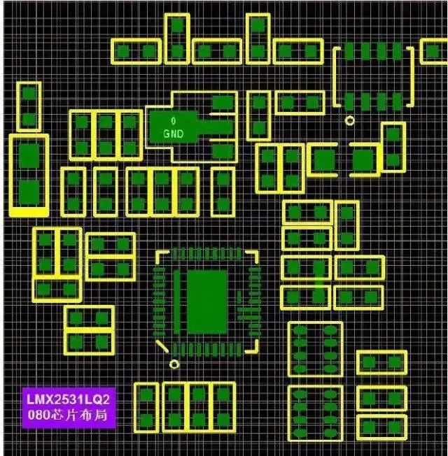
LMX2531LQ2080 chip layout example
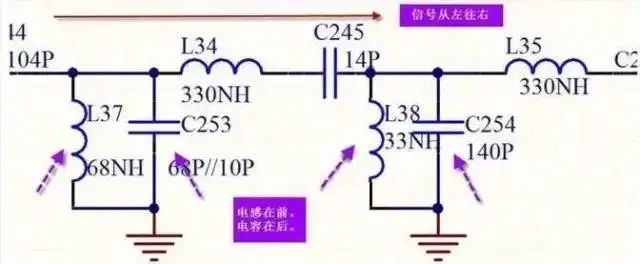
3. Routing Guidelines
- Use 50 Ω impedance trace width with inner‑layer reference.
- Route from pad centers, keep straight, and prefer top layer.
- Bends: Use 45° or arc; avoid right angles.
- Use resistor/capacitor pads as turning points.
- Follow datasheet length and shape for matching traces.
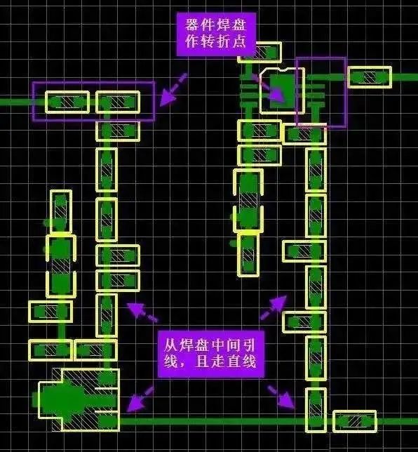
Routing example: center‑fed straight trace with pad‑based turning points
General High‑Frequency Routing Rules
- Layer selection: Use inner planes for GND/power to reduce parasitics and interference.
- Bends: 45° or arc to minimize radiation, coupling, and reflection.
- Length: Keep traces as short as possible.
- Vias: Minimize via count.
- Direction: Route layers perpendicularly (top horizontal, bottom vertical).
- Copper pour: Add GND copper to reduce crosstalk.
- Guard tracing: Guard critical signals with GND.
- Loop avoidance: Use daisy‑chain routing; eliminate loops.
4. Grounding Rules
4.1 RF Chain Grounding
- Use multi‑point grounding.
- Copper gap: 20–40 mil.
- Place GND vias on both sides at uniform spacing.
- Place GND vias near decoupling caps/resistors and component ground pads.
- Recommended via pitch: 60–80 mil.
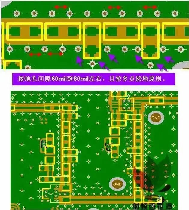
RF chain multi‑point grounding diagram
4.2 Cavity Shell Ground Vias
- Use two staggered rows of vias for better contact.
- Solder mask opening at PCB–cavity contact areas (not on signal traces).
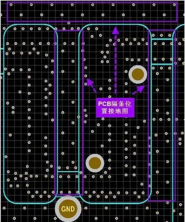
Grounding at PCB partition positions; bottom copper exposure for baseplate contact
4.3 Screw Placement
- PCB–cavity: Place screws at cavity intersections; four corners mandatory.
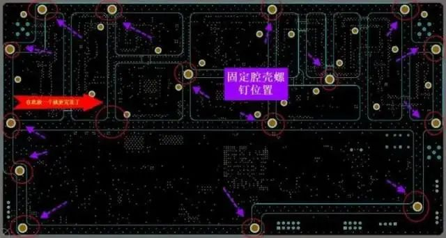
- Screw positions for cavity fastening
- PCB–baseplate: At least one screw per cavity; add at corners; place near SMA/connectors to prevent board flex.
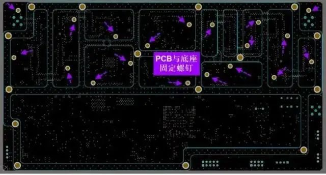
- Screw layout inside cavities
About Maxipcb
Maxipcb empowers innovators to turn cutting-edge technologies into reality.
We offer one-stop solutions for design, simulation, testing, PCB manufacturing, component procurement and SMT assembly, enabling efficient development, rapid deployment and risk control across the full product lifecycle.
Serving the world in communications, industrial automation, aerospace, automotive, semiconductor and beyond, we build a safer, more connected future together.


