Definition of HDI (per IPC-2226)
- PCB trace width and spacing ≤ 100 μm
- Via diameter ≤ 150 μm and pad size < 400 μm
- Higher connection pad density than conventional PCBs (> 20 pads/cm²)
Definition of Microvia (per IPC-2226)
- Pad diameter ≤ 350 μm
- Plated hole diameter ≤ 150 μm, formed by laser or mechanical drilling
- Aspect ratio (depth/diameter) = 1:1 (typical PTH aspect ratio is 10:1)
Common Via Types
- Plated Through Hole (PTH): Through via from outer layer to outer layer
- Blind via: From outer layer to inner layer
- Buried via: Between inner layers only
Via Aspect Ratio (AR)
The ratio of via depth to via diameter.
- PTH: typically 6:1 to 10:1
- 10:1 is the practical limit (lower reliability)
- 6:1 is recommended for best reliability
- Thicker board requires larger via size
Example:
- 1.60 mm board, 0.40 mm via → 4:1
- 1.60 mm board, 0.20 mm via → 8:1
Microvia Features
- Aspect ratio: 1:1 / 1:0.8
- Staggered microvias
- Copper-filled (via-in-pad)
- Stacked microvias
- Skip microvias
- Buried microvias
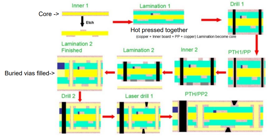
HDI PCB Manufacturing Flow
General process:
Copper etching → Lamination → Drilling → Plating
- Core etching
- Lamination 1 (hot press: copper + inner board + PP + copper)
- Drill 1
- Buried via filling
- Lamination 2
- Drill 2 + Laser drill 1
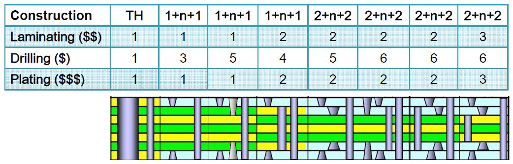
HDI Stage Definition
The “stage” in HDI refers to laser drilling stages.
 About Maxipcb
Maxipcb empowers innovators to turn cutting-edge technologies into reality.
We offer one-stop solutions for design, simulation, testing, PCB manufacturing, component procurement and SMT assembly, enabling efficient development, rapid deployment and risk control across the full product lifecycle.Serving the world in communications, industrial automation, aerospace, automotive, semiconductor and beyond, we build a safer, more connected future together.