To learn high-speed PCB design, the first thing to understand is what a transmission line is. Signal reflection occurs because the traces on the PCB have a certain impedance, and the impedance mismatch between the line impedance and the output impedance will lead to signal reflection. Signal transmission in the PCB will cause delay, and if the timing is not matched, the system will fail to operate. All these problems are caused by transmission lines.
To learn high-speed PCB design, the first thing to understand is what a transmission line is. Signal reflection occurs because the traces on the PCB have a certain impedance, and the impedance mismatch between the line impedance and the output impedance will lead to signal reflection. Signal transmission in the PCB will cause delay, and if the timing is not matched, the system will fail to operate. All these problems are caused by transmission lines.
What is a Transmission Line?
A transmission line is defined as a signal line with a signal return path (consisting of two conductors of a certain length: one is the signal propagation path, and the other is the signal return path). The most common transmission lines are the traces on our PCB boards.
- When analyzing a transmission line, it is essential to associate it with the return path; a single conductor cannot form a transmission line.
- Like resistors, capacitors, and inductors, a transmission line is also an ideal circuit component, but its characteristics are quite different. It delivers good performance in simulation, but its circuit concept is relatively complex.
- A transmission line has two very important characteristics: characteristic impedance and time delay.
Concept and Structural Analysis of Transmission Lines in High-Speed PCB Design
Transmission Line Impedance
First, let's clarify several concepts: we often see impedance, characteristic impedance, and instantaneous impedance. Strictly speaking, they are different, but they all follow the basic definition of impedance without exception.
- The input impedance at the beginning of the transmission line is referred to as impedance for short.
- The instantaneous impedance encountered by the signal at any moment during propagation is called instantaneous impedance.
- If a transmission line has a constant and unchanging instantaneous impedance, it is called the characteristic impedance of the transmission line.
Characteristic impedance describes the transient impedance experienced by the signal as it propagates along the transmission line, which is a major factor affecting signal integrity in transmission line circuits.
Unless otherwise specified, characteristic impedance is generally used to collectively refer to transmission line impedance.
Transmission Time Delay
Time delay (TD) usually refers to the time taken for an electromagnetic signal or optical signal to pass through the entire transmission medium. For a transmission line, the time delay refers to the time taken for the signal to pass through the entire transmission line.
Propagation delay (PD) usually refers to the time delay of an electromagnetic signal or optical signal propagating in a unit length of transmission medium, which is inversely proportional to the "propagation speed", with the unit of "ps/inch" or "s/m".
It can be seen from the definition that Time Delay = Propagation Delay × Transmission Length (L).
Transmission Line Structures in PCB
The transmission line structures seen in a typical PCB are composed of conductors embedded in or adjacent to a dielectric or insulating material, with one or more reference planes. The metal used in a typical PCB is copper, and the dielectric is a fiberglass material called FR4. The two most common transmission line types in digital design are microstrip lines and striplines.
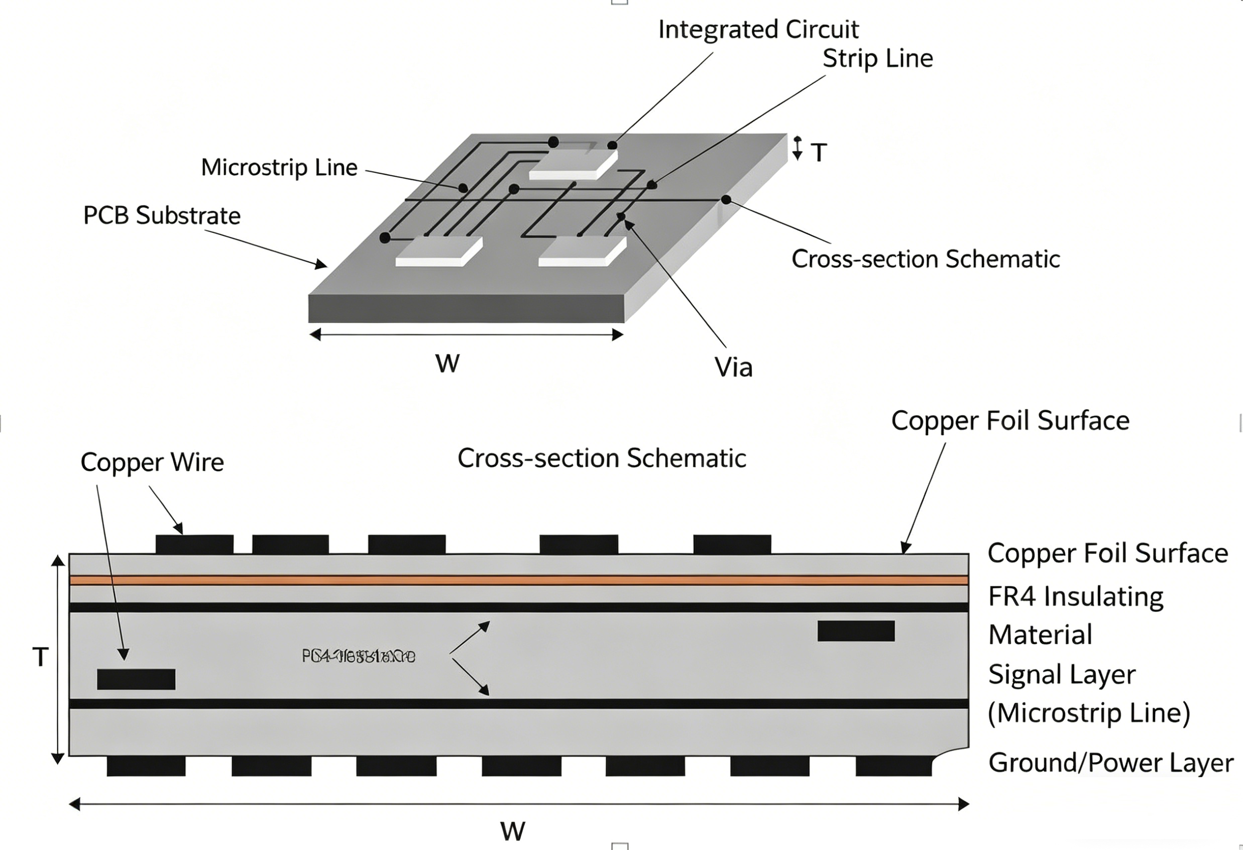
A microstrip line usually refers to a trace on the outer layer of the PCB, with only one reference plane. There are two types of microstrip lines: embedded and non-embedded. An embedded (sometimes referred to as submerged) microstrip line is a transmission line simply embedded in the dielectric, but it still has only one reference plane. A stripline refers to an inner layer trace sandwiched between two reference planes.
The figure below shows the inner layer traces (striplines) and outer layer traces (microstrip lines) between different components on the PCB. The cross-sectional view at the marked position shows the relative relationship between the transmission lines and the ground/power layers.
 About Maxipcb
Maxipcb empowers innovators to turn cutting-edge technologies into reality.
We offer one-stop solutions for design, simulation, testing, PCB manufacturing, component procurement and SMT assembly, enabling efficient development, rapid deployment and risk control across the full product lifecycle.Serving the world in communications, industrial automation, aerospace, automotive, semiconductor and beyond, we build a safer, more connected future together.
