• Multilayer PCB
  • Multilayer PCB
  • Multilayer PCB
  • Multilayer PCB
  • Multilayer PCB
  • Multilayer PCB

Multilayer PCB

Product Model: Multilayer Printed Circuit Board (PCB)

Substrate Material Options: KB6061, S1141, S1000, IT180 (high-performance resin substrates, compliant with PCB industry material standards)
Layer Configuration: 4-layer to 48-layer multilayer PCB, supporting customized layer design based on application requirements
Solder Mask Color: Green, White, Blue, Red (standard color options; custom colors available upon request)
Silk Screen Color: White, Black (high-contrast silk screen for clear component identification and assembly guidance)
Finished Board Thickness: 0.3 mm to 6.0 mm, with precise thickness control to meet diverse mechanical and electrical requirements
Copper Weight: 0.5 oz to 6 oz (17 μm to 170 μm), adaptable to different current-carrying and heat dissipation needs
Surface Finish Options: Immersion Gold (ENIG), OSP (Organic Solderability Preservative), Lead-Free HASL (Hot Air Solder Leveling), ensuring excellent solderability and corrosion resistance
Minimum Trace Width: 3 mil (0.076 mm), achieving high circuit density and precise signal transmission
Minimum Trace Spacing: 3 mil (0.076 mm), effectively preventing signal crosstalk and ensuring electrical insulation reliability
Target Application Field: Consumer Electronics (including but not limited to smart devices, home appliances, portable electronics, and digital products)

  • Multilayer PCB
  • Multilayer PCB
  • Multilayer PCB
  • Description

  • Data Sheet

Product Description

Functional Adaptability for Complex Electronics

The 4-48 layer multilayer pcb is engineered to address the evolving complexity demands of modern electronic systems, targeting industries requiring high-density and multi-functional circuit boards. Its scalable layer configuration from 4 up to 48 layers supports sophisticated routing and circuit density strategies crucial for advanced device manufacturers. This flexibility ensures compatibility with diverse user requirements, making it an essential component for businesses needing reliable pcb assembly services or a trusted pcb assembly manufacturer capable of delivering tailored pcb solutions. Such products benefit from enhanced electrical performance suited to rapid prototyping and volume production alike.

Technical Specifications Ensuring Precision and Reliability

Manufactured according to strict IPC standards, the multilayer pcb incorporates high-performance substrates such as KB6061 and IT180 to optimize mechanical stability and signal integrity. Key features include a minimum trace width and spacing of 3 mil (0.076 mm), multiple surface finish options like Immersion Gold (ENIG), OSP, and Lead-Free HASL, and board thickness controlled between 0.3 mm to 6.0 mm. These specifications enable consistent impedance control and reduced crosstalk, critical for meeting demanding electrical performance criteria. The product integrates power and ground planes internally for stable power distribution, thereby supporting precise pcb prototype service and custom pcb assembly requirements.

Industry Applications Emphasizing Performance and Integration

This multilayer pcb finds extensive application across consumer electronics, telecommunications, and industrial automation sectors where complex multilayer routing and signal integrity are paramount. It facilitates the development of miniaturized smart devices and high-performance electronic assemblies requiring enhanced electromagnetic compatibility. By providing superior solderability and corrosion resistance, the pcb solution supports seamless integration into automated manufacturing lines. Professional pcb assembly manufacturers rely on this multilayer pcb to deliver consistent quality, contributing to improved system reliability and return on investment in product development cycles.


Product Advantages

Design Flexibility and System Integration

The multilayer pcb’s configurable design from 4 to 48 layers permits modular integration tailored to specific electrical and mechanical specifications, addressing variation in power distribution and signal routing efficiently. Its compatibility with multiple solder mask colors and silk screen options enhances visual component identification during assembly. The layered architecture allows embedding of power and ground planes internally, improving electromagnetic compatibility and noise reduction. Such features reflect the capabilities of a sophisticated pcb assembly manufacturer or service provider delivering custom pcb assembly projects aligned with precise client specifications.

Optimized Performance and Operational Efficiency

From a performance standpoint, this multilayer pcb ensures reliable operation with copper weight options ranging from 0.5 oz to 6 oz, enhancing current capacity and heat dissipation. Its fine pitch capabilities with minimum trace width and spacing down to 3 mil enable high-density circuit layouts required in advanced electronics. These attributes contribute to manufacturing efficiency by reducing defects and rework, making it suitable for comprehensive pcb assembly services. End users benefit from enhanced product durability and reduced electromagnetic interference, ultimately promoting better system functionality and lifecycle management within pcb solutions.


Multilayer PCB Stack-Up Design

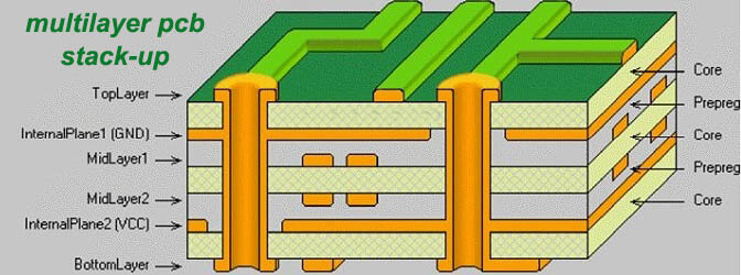
Multilayer PCB stack-up is a critical design link that directly affects the electrical performance, signal integrity, and manufacturing feasibility of the board. The stack-up layout typically arranges surface layers on both sides of the PCB, with internal layers including power supply layers, ground layers, and signal layers. Rational stack-up design can effectively reduce signal crosstalk, improve electromagnetic compatibility (EMC), and optimize heat dissipation performance.

Maxipcb: Professional Multilayer PCB Manufacturer

Maxipcb is a professional manufacturer specializing in multilayer PCB production. We provide high-volume multilayer PCB manufacturing services, offering cost-effective and high-quality multilayer PCBs. Our services include high-quality multilayer PCB prototyping, tailored to meet customer-specific requirements and deliver satisfactory prototyping solutions.

Overview of Multilayer PCBs

A multilayer PCB (Printed Circuit Board) is defined as a circuit board featuring three or more conductive layers. In practical design and manufacturing, multilayer PCBs are typically fabricated with an even number of layers, hence commonly referring to 4-layer, 6-layer, 8-layer, and higher-layer configurations.
Constructed with multiple layers of copper foil conductive layers, the copper foil serves as the circuit layer for the multi-surface circuit board. Different conductive layers are laminated and bonded together, with thermally protected insulating layers separating each layer. The stack-up design of multilayer PCBs ensures that both sides of the board serve as surface layers, while through-holes are utilized to achieve electrical interconnection between different circuit layers. Driven by the continuous upgrading of the electronics industry, the demand for multilayer PCBs has grown significantly to meet the evolving requirements of advanced electronic products.
The continuous advancement of SMT (Surface Mount Technology) and the introduction of new-generation SMDs (Surface Mount Devices)—such as QFP (Quad Flat Package), QFN (Quad Flat No-lead Package), CSP (Chip Scale Package), and BGA (Ball Grid Array), particularly MBGA (Micro Ball Grid Array)—have driven the intelligence and miniaturization of electronic products, prompting a major transformation and progress in PCB industrial technology. Since IBM successfully developed high-density multilayer PCBs in 1991, manufacturers worldwide have developed a variety of high-density multilayer circuit boards. The rapid development of multilayer PCB manufacturing technology has guided multilayer PCB design toward high-density routing. Due to its flexible design, stable and reliable electrical performance, and superior economic benefits, multilayer PCBs are widely used in the production of electronic products.
Since the mid-to-late 1980s, the output value of multilayer PCBs has maintained an annual growth rate of over 10%. Driven by the trend of components becoming "lighter, thinner, shorter, and smaller," multilayer PCBs have emerged as the most influential and dynamic category in the PCB industry, becoming the leading product segment. The structure of multilayer PCBs is evolving toward diversification, thinness, and high layer counts. Multilayer PCB production requires significant investment in equipment and technology; in the future, manufacturers will continue to introduce advanced manufacturing equipment, with high-end multilayer PCBs being produced by enterprises with strong technical capabilities.


multilayer PCB stack-up

Development Trends of Multilayer PCBs

  • High Density: Continuous improvement in routing density to accommodate more components and complex circuits within limited board space.
  • Thin and Ultra-High Layer Count: Development toward thinner board profiles and higher layer counts (e.g., 48-layer and above) to meet the miniaturization and high-performance requirements of electronic products.
  • Structural Diversification: Emergence of diverse structures such as rigid-flex multilayer PCBs and HDI (High-Density Interconnect) multilayer PCBs to adapt to complex product designs.
  • High-Performance Thin Copper Substrates: Adoption of thin-base materials with thin copper foils to enhance signal transmission performance and reduce signal loss.
  • High Flatness and Advanced Surface Coating: Improvement of PCB surface flatness and adoption of high-reliability surface coating technologies to ensure solderability and corrosion resistance.
  • Flexible and Rigid-Flex Multilayer PCBs: Growing demand for flexible and rigid-flex multilayer PCBs to adapt to wearable devices and products with complex spatial layouts.

Differences Between Single-Layer, Double-Layer, and Multilayer PCBs

The key distinction between multilayer PCBs and single-layer/double-layer PCBs lies in the addition of internal power supply layers and ground layers. Power supply and ground networks are primarily routed on the internal power supply and ground layers, while signal routing for multilayer PCBs is mainly conducted on the top and bottom surface layers, supplemented by middle signal layers. As a result, the design method of multilayer PCBs is basically consistent with that of double-layer PCBs, with the core focus being the optimization of internal power/ground layer routing to achieve more reasonable PCB layout and better electromagnetic compatibility (EMC).

Multilayer PCB Manufacturing Process

Standard Manufacturing Process (HASL/Immersion Gold Multilayer PCBs)

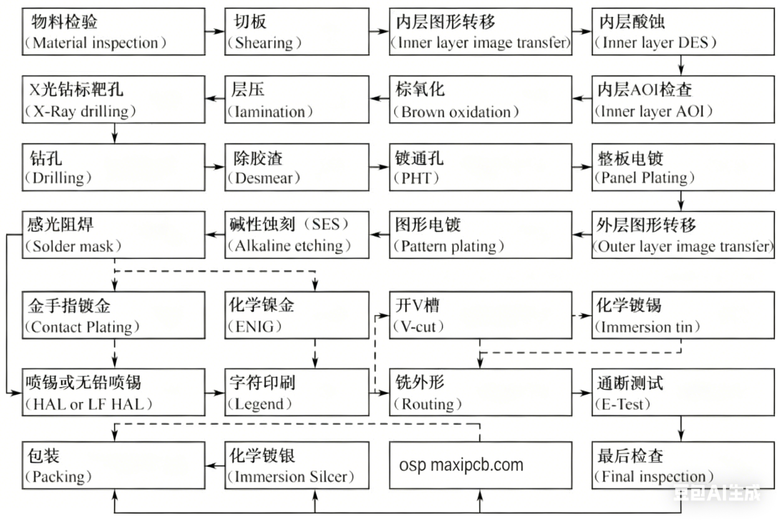
The standard manufacturing process for multilayer PCBs includes the following steps: Material Preparation → Inner Layer Fabrication → Drilling → Copper Deposition → Circuit Patterning → Electroplating → Etching → Solder Mask Application → Silkscreen Printing → Hot Air Solder Leveling (HASL) or Immersion Gold → Routing/Edge Trimming → V-Cutting (if required) → Electrical Testing → Vacuum Packaging.

Gold-Plated Multilayer PCB Manufacturing Process

The manufacturing process for gold-plated multilayer PCBs is as follows: Cutting → Inner Layer Fabrication → Drilling → Copper Deposition → Circuit Patterning → Electroplating → Gold Plating → Etching → Solder Mask Application → Silkscreen Printing → Routing/Edge Trimming → V-Cutting → Electrical Testing → Vacuum Packaging.
Multilayer PCB production requires not only substantial investment in technology and equipment but also extensive experience of technicians and production personnel. Compared with traditional PCBs, multilayer PCBs have higher processing difficulty and stricter requirements for quality and reliability. The following sections detail the key processes and technical points of multilayer PCB manufacturing.

Key Technical Points in Multilayer PCB Manufacturing

1. Material Selection for Multilayer PCBs

With the trend of electronic components toward high performance, multifunctionality, and high frequency, and the rapid development of signal transmission technology, electronic circuit materials are required to have low dielectric constant (Dk), low dielectric loss (Df), low coefficient of thermal expansion (CTE), low water absorption, and high performance. High-quality copper-clad laminates that meet these requirements are essential to ensure the processing feasibility and reliability of multilayer PCBs.

2. Multilayer PCB Stack-Up Design Principles

The core factors to consider in multilayer PCB stack-up design include material heat resistance, voltage resistance, resin filling capacity, and dielectric layer thickness. The following principles must be followed:
  • The prepreg must be from the same manufacturer as the core board to ensure compatibility and bonding reliability.
  • For customer requirements of high-Tg (glass transition temperature) boards, both the core board and prepreg must use corresponding high-Tg materials.
  • For inner core boards with copper weight of 3 oz and above, prepregs with high resin content should be selected to ensure sufficient filling and bonding strength.
  • In the absence of special customer requirements, the dielectric layer thickness tolerance is generally controlled within ±10%; for impedance-controlled boards, the dielectric thickness tolerance shall comply with IPC-4101C/M standards.

3. Inter-Layer Alignment Control

Precise control of inner core board size compensation and production dimension accuracy is critical. Through production data collection and historical experience accumulation, the graphic dimensions of each layer of the multilayer PCB are accurately compensated to ensure consistent expansion and contraction of the core board, thereby guaranteeing inter-layer alignment precision.

4. Inner Circuit Fabrication Technology

To improve the graphic resolution of inner circuits, laser direct imagers (LDI) are widely adopted in multilayer PCB production. In engineering design, appropriate compensation is applied to line width and pads to ensure the accuracy of inner line width, line spacing, isolation ring size, independent lines, and hole-to-line distance. If the design compensation is unreasonable, engineering design adjustments are required.

5. Lamination Process

Current inter-layer positioning methods for multilayer PCB lamination mainly include four-slot positioning (PinLAM), hot melting, riveting, and a combination of hot melting and riveting. Different product structures adopt corresponding positioning methods to ensure lamination accuracy.

6. Drilling Technology

Due to the multiple layers of substrate and copper foil stacked together, the total thickness of the board is relatively large, which causes significant wear to the drill bit and increases the risk of drill breakage. To address this, the drilling speed and rotation speed must be reasonably adjusted based on the number of holes and board thickness.

Multilayer PCB Classification & Pricing Basis

Traditional PCBs are divided into single-layer and double-layer routing configurations, corresponding to single-layer and double-layer PCBs. However, due to product space design requirements, electronic products can adopt multi-layer stacking in addition to surface routing. During the production process, after fabricating each layer of the circuit, optical equipment is used for positioning and lamination, integrating multiple layers of circuits onto a single PCB—commonly referred to as a multilayer PCB. Any circuit board with three or more layers is classified as a multilayer PCB.
Multilayer PCBs can be divided into rigid multilayer PCBs, flexible multilayer PCBs, and rigid-flex multilayer PCBs. The manufacturing price of multilayer PCBs is calculated based on the PCB area and the difficulty of the manufacturing process.

Application Scenarios of Multilayer PCBs

1. Application in Compact Consumer Electronics Manufacturing

In the manufacturing of miniaturized consumer electronics such as smartphones, wearables, and smart home devices, multilayer PCBs provide the high-density electrical routing required for complex functionality within limited form factors. Their thin profile and reliable via interconnections are compatible with SMT and SMD components (e.g., QFP, BGA), which are critical for advanced device assemblies. By integrating with PCB prototype services, R&D teams can rapidly iterate on multilayer designs, accelerating product validation and production readiness. This solution ensures compliance with thermal and mechanical standards, maintaining product reliability in demanding consumer application scenarios.

2. Role in Industrial Control and Automation Systems

In industrial control and automation systems, where reliability and precision are paramount, multilayer PCBs serve as the backbone for robust signal routing and power distribution. The multilayer configuration supports diverse control circuitry with the electromagnetic compatibility and thermal resilience required in harsh industrial environments. As part of custom PCB assembly workflows, these boards are fabricated to strict tolerances, ensuring seamless integration with sensors, actuators, and communication modules. Advanced surface treatments protect against industrial contaminants, maintaining long-term stability essential for continuous production and system uptime.

Frequently Asked Questions (FAQ)

Q1: What materials are commonly used for multilayer PCB manufacturing?

A1: Multilayer PCBs are typically manufactured using high-performance substrate materials such as KB6061, S1141, S1000, and IT180. These materials offer excellent electrical insulation and mechanical stability, supporting the reliable performance of complex multilayer designs required by PCB assembly services.

Q2: Can multilayer PCBs be customized to specific electrical and mechanical requirements?

A2: Yes, multilayer PCBs can be fully customized, including layer counts ranging from 4 to 48, various copper thicknesses, solder mask colors, and surface treatments (e.g., Immersion Gold, HASL). This flexibility caters to the custom specifications commonly required in PCB prototype services and advanced electronic assemblies.

Q3: How does Maxipcb ensure quality and reliability in PCB production?

A3: Maxipcb implements a rigorous quality management system certified to ISO9001, RoHS, and UL standards. Production strictly adheres to IPC standards, supported by precision testing equipment and a skilled technical team, ensuring every multilayer PCB meets customer requirements and industry compliance.

Q4: What support is available for integrating multilayer PCBs in electronic assemblies?

A4: Maxipcb provides comprehensive support as a PCB assembly manufacturer, including design consultation for SMT and SMD components, precise layer stack-up design, and advanced surface treatments. This service helps optimize PCB integration to ensure stable electrical performance in complex electronic products.


What substrate materials are used in your multilayer pcb production?
We use industry-standard high-performance resins including KB6061, S1141, S1000, and IT180 as substrates. These materials ensure mechanical stability and electrical reliability for your multilayer pcb needs, supporting various applications to guarantee durability and performance.

Can Maxipcb customize multilayer PCBs for specific electrical and mechanical requirements?
Yes, we offer fully customizable multilayer pcb solutions with layer counts from 4 to 48, adjustable thickness, copper weights, solder mask and silk screen colors, and surface finishes. This flexibility allows us to meet your unique project specifications precisely.

Do you provide services for quick prototyping and small batch production?
We support pcb prototype service and small-to-large batch manufacturing using advanced fabrication processes and experienced teams. This ensures your multilayer PCBs maintain consistent quality while accommodating development timelines and volume demands.

How does Maxipcb handle logistics and quality assurance for international clients?
Our facility is ISO and IPC standard compliant, with rigorous quality control throughout production. We maintain a global sales network and reliable logistics channels to deliver your multilayer pcb orders efficiently, ensuring professional pcb assembly manufacturer support worldwide.

Model: Multilaver PCB

Material:KB6061.S1141.S1000.1T180

Layer: 4Layer -48Layer Multilayer PCB

Solder Mask Color: Green/white/Blue/Red

Silk Screen Color: White/Black

Finished Thickness: 0.3mm -6.0mm

Copper Thickness: 0.5-6OZ

Surface Treatment: lmmersion Gold/OSP/HASL

Min Trace: 3mil(0.75mm)

Min Space: 3mil(0.75mm)

Application: Consumer electronics