As the name implies, a thick copper PCB is a printed circuit board with a thicker copper conductive layer. Some manufacturers distinguish PCBs with a copper thickness of ≥2oz from standard boards and define them as thick copper PCBs.
PCB fires, component smoking, and even explosions are common issues for many electronic engineers, especially for power boards carrying high currents—with high voltage and large current, they are extremely prone to fire risks. So how to avoid such failures? For such scenarios, the optimal solution is to adopt thick copper PCB design.
What Is a Thick Copper PCB?
As the name implies, a thick copper PCB is a printed circuit board with a thicker copper conductive layer. Some manufacturers distinguish PCBs with a copper thickness of ≥2oz from standard boards and define them as thick copper PCBs. (There is no unified industry standard at present; however, in the 4th draft of Terms and Definitions for Electronic Circuit Industry issued by CPCA (China Printed Circuit Association) in 2021 for public comment, a thick copper PCB is defined as: a printed circuit board (including single-sided, double-sided, and multilayer boards) with a copper thickness of the conductive pattern exceeding 105μm (3oz)).
Why Thick Copper PCBs Are Required for High-Current Applications
First, thick copper PCBs feature high current carrying capacity
According to the formulas:

(Where
I = load current,
U = voltage,
R = resistance,
S = cross-sectional area of the trace,
\(\rho\) = resistivity,
L = trace length,
w = trace width,
h = trace thickness)
It can be concluded that under fixed conditions (especially trace width), the load current I of the trace is directly proportional to the trace thickness h. The thicker the trace, the larger the current it can carry.
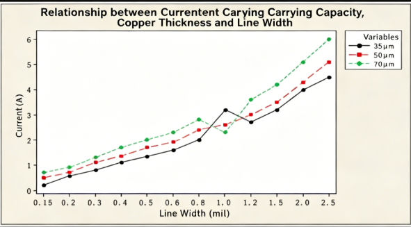
Relationship between Current Carrying Capacity, Copper Thickness and Trace Width
(Variable: 35μm/50μm/70μm copper thickness; Horizontal axis: Trace width (mil); Vertical axis: Current carrying capacity (A))
Second, thick copper PCBs provide excellent heat dissipation performance
Metal core PCBs, typically aluminum-based and copper-based PCBs, are well known for their outstanding heat dissipation performance. Thick copper PCBs also achieve favorable heat dissipation capability due to their relatively thick copper layers.
The following is a set of experimental data on the influence of copper foil thickness on heat dissipation:
Test setup: 5×5mm copper sheet, aluminum substrate, copper foil; single variable method (gradually increasing copper foil thickness) to measure the temperature difference between two end faces of the copper foil.
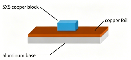
Experimental Curve of Copper Foil Thickness Effect on Heat Dissipation
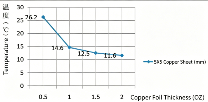
The curve shows that the temperature difference between the two end faces of the test sample gradually decreases as the copper foil thickness increases.
Therefore, adopting thick copper PCB design can improve the heat dissipation performance of the board.
Third, thick copper PCBs reduce thermal strain
According to the heat generation formula:

(Where
Q = heat generation,
I = passing current,
R = resistance,
t = energizing time,
\(\rho\) = resistivity,
L = trace length,
S = cross-sectional area,
w = trace width,
h = trace thickness)
It can be concluded that under fixed conditions, the heat generation of the trace is inversely proportional to the trace thickness.
Therefore, thick copper PCB design reduces heat generation, thereby mitigating thermal strain caused by heat accumulation.
In summary, unlike standard PCBs, thick copper PCBs have three prominent advantages: high current carrying capacity, excellent heat dissipation, and reduced thermal strain, which greatly lower the risk of board burnout, making them an ideal choice for high-current PCB design. In addition, thick copper PCBs can enhance the mechanical strength of the circuit board and reduce the volume of end products.
About Maxipcb
Maxipcb empowers innovators to turn cutting-edge technologies into reality.
We offer one-stop solutions for design, simulation, testing, PCB manufacturing, component procurement and SMT assembly, enabling efficient development, rapid deployment and risk control across the full product lifecycle.Serving the world in communications, industrial automation, aerospace, automotive, semiconductor and beyond, we build a safer, more connected future together.
