
RF PCB · On‑Board Antenna · Keep‑Out Area
An on‑board antenna works together with surrounding copper, components, and mechanical structures. The keep‑out region must be managed as part of the overall system.
Placing a PCB antenna at the edge of the board is only the starting point. The copper, traces, components, battery, enclosure, cables, and even the user's hand all change the electromagnetic environment around the antenna. The keep‑out area should span the specified layers and maintain structural stability. Final matching must always be verified in the fully assembled product.
On the same wireless board, the bare board may show a good connection during stand‑alone testing. But after inserting the battery and closing the enclosure, the communication distance shortens, throughput drops, or the frequency shifts. A layout review may show that the top layer already has no copper around the antenna.
The problem may lie in interpreting the keep‑out area as simply "a blank region on the top layer." An on‑board antenna is not an isolated copper trace. Together with the feed line, reference ground, all adjacent layers, and the overall mechanical assembly, it forms an electromagnetic system.
1. Why Is a PCB Antenna So Sensitive to Its Surroundings?
An on‑board antenna radiates through its current distribution and the surrounding electromagnetic field. Nearby conductors, dielectrics, and metal structures change the equivalent capacitance, inductance, losses, and current paths, which in turn can shift resonance, matching, and efficiency.
This is why the same antenna trace cannot be assumed to perform identically when placed on different board outlines, materials, ground sizes, or enclosures. Reference‑design dimensions are meaningful only under similar boundary conditions.
2. Why Must the Keep‑Out Area Be Examined Across All Relevant Layers?
If an inner ground plane, signal traces, or power copper exists directly beneath the top‑layer antenna, the electric field distribution will differ from the reference structure. The keep‑out area should typically follow the antenna or chip vendor's reference design, restricting copper, traces, vias, and components within the specified layers.
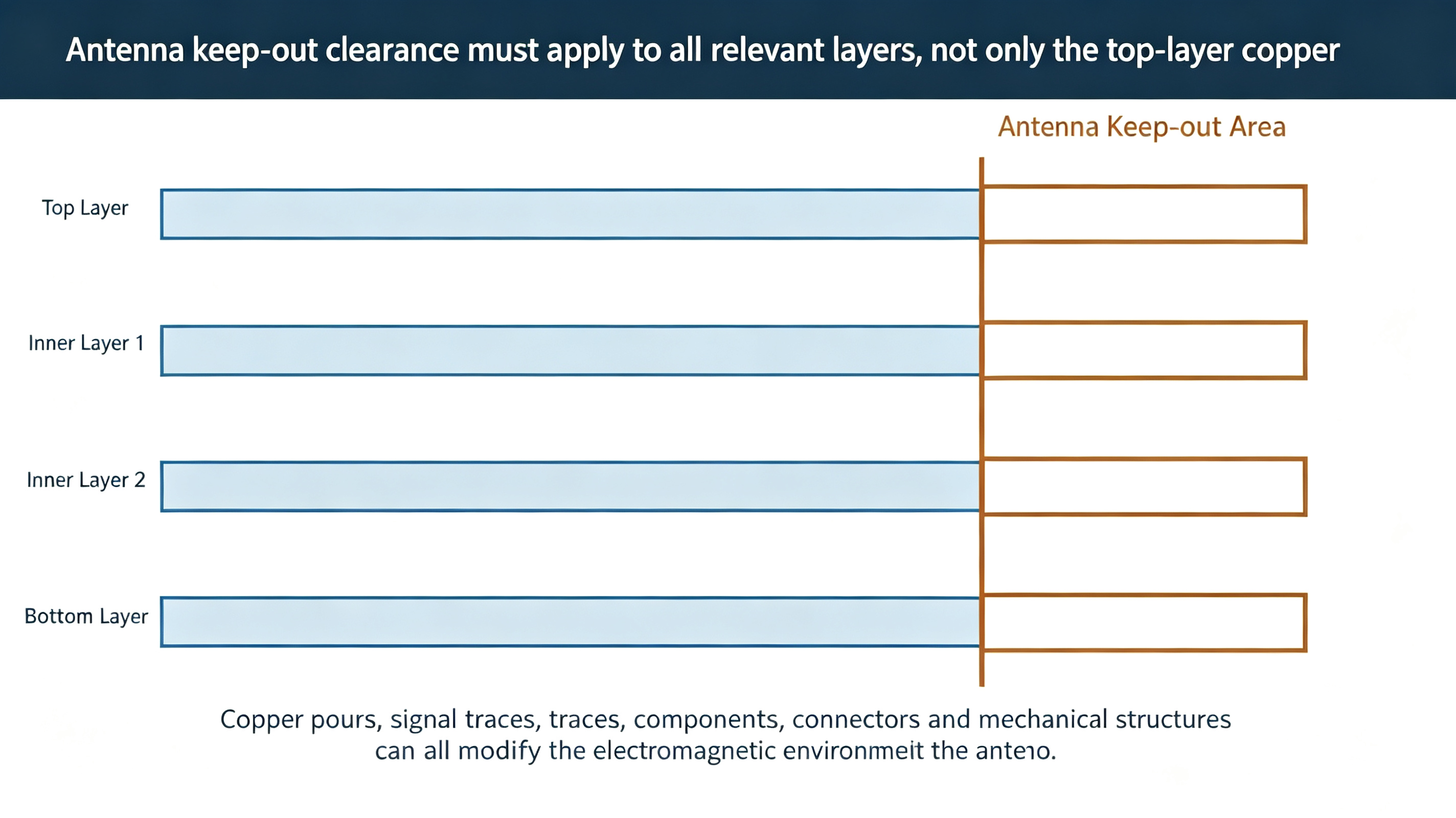
Figure 1 – The antenna keep‑out should extend across the relevant layers specified in the reference design (schematic illustration, not actual measurement results).
The exact shape and number of keep‑out layers cannot be generalised from experience alone; they must be based on the specific antenna, board thickness, material, and vendor guidelines. The key point of this article is the inspection method: do not simply switch to the top layer and take a quick look.
3. Why Does Detuning Most Often Occur After Enclosure Assembly?
The battery, display, metal brackets, shielding cans, coating on the enclosure, connectors, and cables all approach the antenna and establish new boundary conditions. The user's hand grip, tabletop placement, and mounting orientation can also change the loading environment.
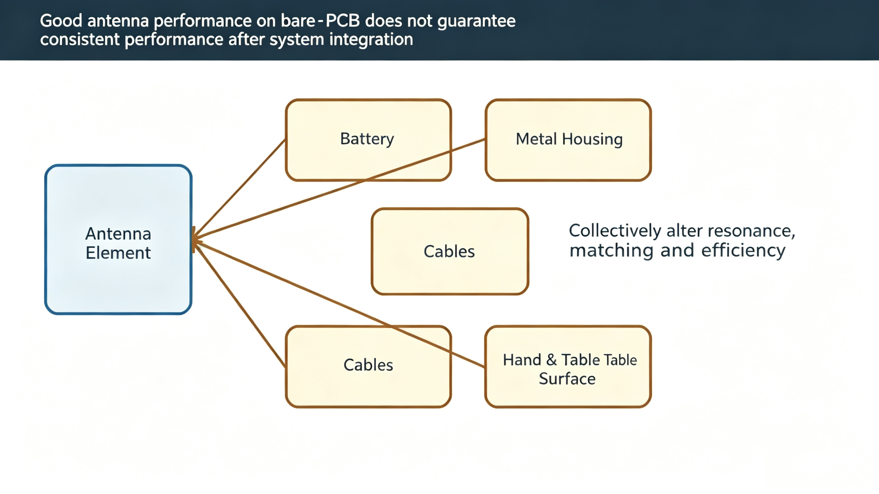
Figure 2 – The battery, enclosure, cables, and usage posture jointly alter the antenna environment (schematic illustration, not actual measurement results).
Therefore, bare‑board matching can only serve as an intermediate result. Final tuning should be re‑measured on production‑intent mechanical assemblies, with typical cables and representative usage postures. If the mechanical structure is still changing, freezing the matching values too early carries significant risk.
4. The Feed Line and Reference Ground Are Also Part of the Antenna
The trace from the RF chip or matching network to the antenna feed point must maintain controlled impedance and a continuous reference plane. An excessively long feed line, crossing a split plane, passing through dense via fields, or experiencing abrupt changes in surrounding copper can introduce loss and mismatch before the signal even reaches the antenna.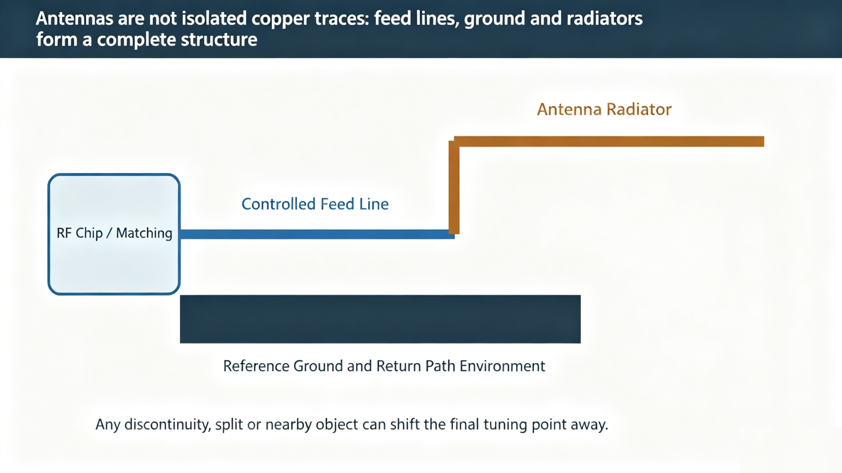
Figure 3 – The feed line, reference ground, and radiating element form a complete structure (schematic illustration, not actual measurement results).
The location of the ground feed point, return vias, and matching components is equally critical. The matching network should be placed as specified and should provide a controlled structure for measurement and tuning. It must not be treated as a few small components that can be placed arbitrarily.
5. From Layout to System Tuning – Follow These 5 Steps
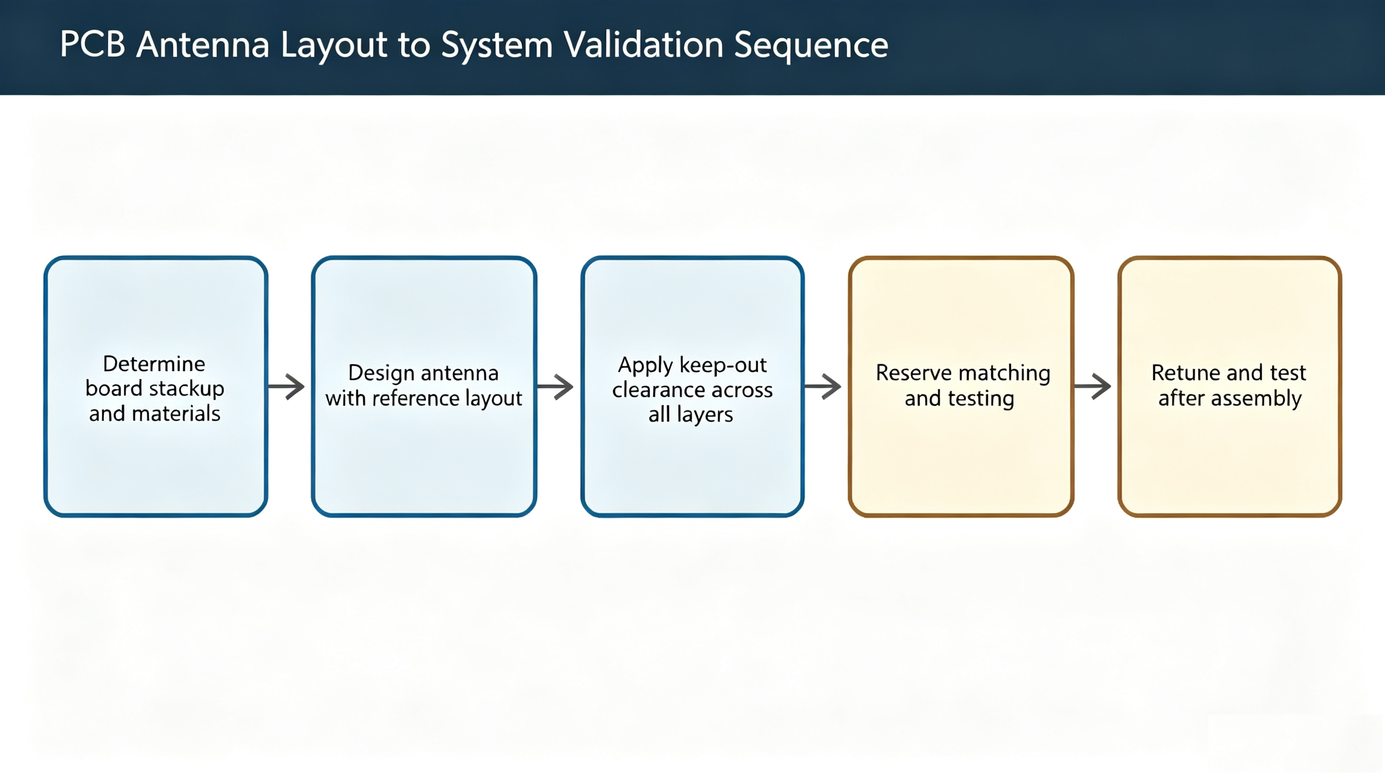
Figure 4 – Sequence from PCB layout to full‑system antenna verification (schematic illustration, not actual measurement results).
-
Lock down the board outline, stack‑up, materials, ground size, and enclosure boundaries. Confirm the applicable conditions for the reference design.
-
Place the radiating element, feed line, ground‑feed point, and matching network according to the antenna or chip vendor's guidelines.
-
Implement the keep‑out on all specified layers, and verify that no components, vias, traces, or copper violate the boundaries.
-
Reserve RF test points and matching locations to avoid using long flying leads during debugging, which would disturb the original structure.
-
Measure return loss, efficiency, or system‑level metrics on the fully assembled product with typical cables and representative usage postures, then perform final matching.
6. Three Common Misconceptions
-
Placing the antenna at the board edge guarantees correct performance. The edge is a common placement but still requires proper ground, keep‑out, and mechanical constraints.
-
No copper on the top layer equals a proper keep‑out. Inner layers, bottom layers, components, and mechanical parts may all enter the field region.
-
Matching capacitors can fix any problem. Matching can only adjust impedance within a certain range; it cannot remedy fundamental radiation‑efficiency or environmental issues.
Engineering Judgement
The keep‑out area for a PCB antenna is an electromagnetic boundary that runs through the stack‑up and the complete mechanical assembly – it is not merely a blank area on the top layer. Final performance must be verified in the fully assembled product; bare‑board results cannot be used as a substitute.
Final Note
The next time the antenna performance degrades after enclosure assembly, do not immediately start swapping matching capacitors. Instead, compare the bare board with the complete assembly side‑by‑side: what new copper, metal, dielectrics, and cables have been introduced around the antenna?
Only when the antenna environment is kept predictable does matching become the final fine‑tuning step. When the environment keeps changing, the tuned values are unlikely to be stable or reusable.
About Maxipcb
We offer one-stop solutions for design, simulation, testing, PCB manufacturing, component procurement and SMT assembly, enabling efficient development, rapid deployment and risk control across the full product lifecycle.
Serving the world in communications, industrial automation, aerospace, automotive, semiconductor and beyond, we build a safer, more connected future together.