To isolate two high‑speed signal lines, a full row of grounding vias was placed between them, with the assumption that crosstalk would be suppressed. But when the isolation was measured, the high‑frequency band showed almost no suppression – the coupling remained strong. Too few vias seemed ineffective, while too many risked wasting space and obstructing routing – so what is the right approach?
To isolate two high‑speed signal lines, a full row of grounding vias was placed between them, with the assumption that crosstalk would be suppressed. But when the isolation was measured, the high‑frequency band showed almost no suppression – the coupling remained strong. Too few vias seemed ineffective, while too many risked wasting space and obstructing routing – so what is the right approach?
How Grounding Vias Work
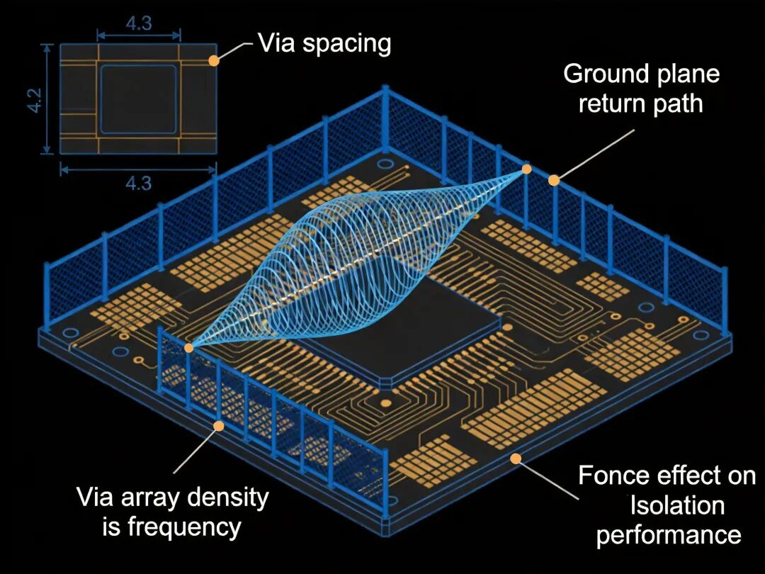
Grounding vias create a "via fence" on the PCB. In essence, they form an artificial ground plane between two signal paths, providing a low‑impedance return path for the coupled electromagnetic field instead of allowing it to couple directly onto adjacent signal traces. However, vias are not infinitely effective – their isolation performance depends on frequency, spacing, and quantity.
At high frequencies, the wavelength of the electromagnetic wave becomes very short. If the via spacing exceeds λ/20, the gaps between vias act as "leakage channels" for the electromagnetic field, causing isolation to degrade sharply. So even if a row of vias is present, if the spacing is too large, high‑frequency leakage will still occur.
Calculating Spacing and Quantity
A rule‑of‑thumb formula for via spacing: spacing ≤ λ/20, where λ is the wavelength of the signal in the dielectric. For example, for a 5 GHz signal, the wavelength in FR‑4 is approximately 30 mm, so the via spacing must not exceed 1.5 mm. If the operating frequency is higher (e.g., above 10 GHz), the spacing should be reduced to less than 1 mm.
However, vias should not be packed too densely either. Over‑dense placement introduces two problems: first, it makes fabrication difficult – the copper between vias becomes too narrow and prone to cracking; second, it encroaches on routing space, forcing high‑speed traces to detour, which introduces impedance discontinuities and reflections. A general recommendation is to keep the spacing at about 2‑3 times the diameter of the signal via. This provides good isolation without excessively consuming board space.
Vias Alone Are Not Enough – Ground Plane Integrity Matters
Many engineers focus solely on the vias between signal lines, overlooking the fact that a solid ground plane is the foundation of isolation. If a row of vias is present but the reference ground plane is fragmented by other vias, pads, or traces, the return path is incomplete. Signals will still take long detours, and coupling will remain strong.
Check method: In your PCB layout tool, open the ground plane layer and look for continuous copper beneath the signal lines. If there are voids, dense via clusters, or split lines under the signal path, the return current will be forced to detour, generating common‑mode radiation and crosstalk.
Solution: When signals change layers – for example, from top to bottom – the reference ground plane must follow. A grounding via must be placed next to the signal via to connect to the inner ground plane, ensuring the shortest possible return path. Do not simply add vias between the signal lines; the reference plane along the entire signal path must also remain intact.
Important Note: Isolation issues are not limited to coupling between signal lines – noise coupling on the power plane is also a concern. If both signal paths share the same ground plane, noise on that plane will couple onto both signals as common‑mode interference. In such cases, vias between signal lines alone will not help. Additional filtering at the power entry point is required, or the two signals should be assigned to different reference layers.
How to Determine Whether the Via Scheme Is Correct
The most direct method is simulation. Use HFSS or CST to build a via‑fence model and sweep frequencies to examine the S‑parameters (S21 represents isolation; lower is better). Simulation quickly reveals the effectiveness of different spacings and row counts, avoiding trial‑and‑error board revisions.
If simulation is not feasible, an empirical approach can be used: first, place one row of grounding vias on each side of the critical signal lines, with spacing calculated as λ/20. The number of vias should cover the entire signal path, including bends. After testing, if isolation is still insufficient, prioritise checking ground‑plane integrity rather than blindly adding more vias.
Practical Case Study
In a dual‑channel RF receiver, three rows of grounding vias with 1 mm spacing were placed between the two channels. However, isolation at 2.4 GHz was only ‑40 dB, far short of the required ‑60 dB. Investigation revealed that the inner ground plane beneath the vias had been fragmented by a cluster of USB interface vias, forcing the signal return current to detour by 15 mm. After adding several grounding vias to bridge the fragmented ground plane, the isolation directly improved to ‑65 dB. Ground‑plane continuity proved far more important than the sheer number of vias.
Conclusion
Insufficient isolation from grounding vias does not necessarily mean too few vias were used; it is more likely that the spacing is too large or the ground plane is incomplete. First, calculate the required via spacing for the operating frequency, then check the continuity of the reference ground plane. Addressing these two steps will resolve the issue.
About Maxipcb
Maxipcb empowers innovators to turn cutting-edge technologies into reality.
We offer one-stop solutions for design, simulation, testing, PCB manufacturing, component procurement and SMT assembly, enabling efficient development, rapid deployment and risk control across the full product lifecycle.
Serving the world in communications, industrial automation, aerospace, automotive, semiconductor and beyond, we build a safer, more connected future together.
