Why Are Some GND Pads Still Not Connected Even Though the Ground Copper Has Clearly Been Poured?
Why Are Some GND Pads Still Not Connected Even Though the Ground Copper Has Clearly Been Poured?
Seeing a large area of ground copper on the PCB does not mean every GND pad is already conductive. Net names, copper pour updates, clearance rules, thermal relief connection methods, and island removal can all cause a pad to look like it is next to copper while actually not being connected.
Sometimes the PCB looks quite normal: the ground copper has been poured, and several GND pads are surrounded by copper color. But when DRC is run, it still reports an unconnected item; or when you zoom in, you find that although there is copper around the pad, a thin gap separates them.
In this situation, do not rush to draw another wire. First confirm whether what you see is “copper poured nearby” or whether the pad is truly connected to the GND net.
First Check the Net Name—Do Not Just Look at “GND” Written Next to the Pad
Copper pour connects objects only according to net rules. If the copper pour’s Net is GND but the pad’s Net is GND_A, AGND, or another net, the software will not automatically connect them just because the names look similar. Incorrect schematic net labels or a package pad that did not correctly inherit the net can also cause similar problems.
First open the problematic pad and check its Net, then open the copper pour and check its Net. Only if the two match should you continue checking the subsequent settings. The text “GND” printed on the PCB does not prove that the pad’s actual net is GND.
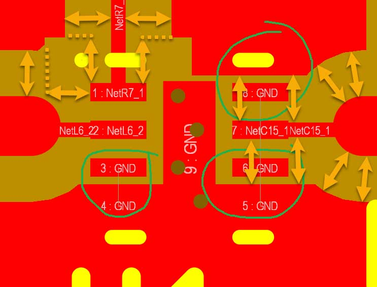
Figure 1: In an actual layout, clearance areas may prevent a GND pad from connecting to nearby copper.
Has the Copper Pour Been Updated? Has the Connection Method Been Set to No Connect?
In EDA tools such as AD, after modifying traces, pads, or copper pour boundaries, you need to repour. Looking only at the old copper pour display can easily lead you to treat outdated copper as the final result.
Pads on the same net usually use thermal relief or direct connect according to the rules. If the rule is set to No Connect, the copper pour will not automatically connect to the pad even if it is right next to it. A thermal relief connection leaves several copper spokes; when zoomed in, the actual connection structure should be visible.
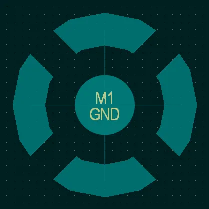
Figure 2: A thermal pad connects to the large copper pour through copper spokes; both the electrical connection and the appearance should be confirmed.
Copper Being Pushed Apart, or Only an Island Remaining, Can Also Cause No Connection
When there are traces, vias, or pads of other nets around the pad, the copper pour must obey electrical clearance. Once clearance cuts the copper plane, an area that looks like one whole piece visually may already be divided into several pieces electrically.
Options such as Remove Dead Copper / Remove Islands clean up isolated copper areas that are not connected to net objects. For GND pours, this is usually worth checking; however, if a copper area has a clear design purpose, do not blindly change settings just to eliminate an error. Also check thermal spoke width, air gap, and surrounding clearance to prevent the connecting spokes from being squeezed out.
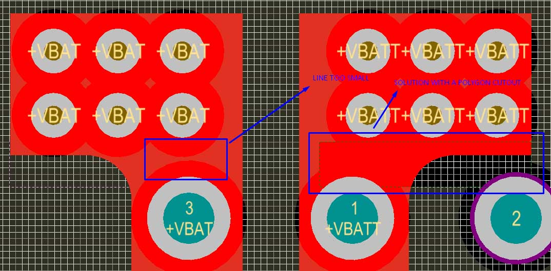
Figure 3: An overly narrow copper neck or an isolated area may be cleaned up; the presence of copper pour does not equal electrical continuity.
My inspection order is generally: confirm the pad Net → confirm the copper pour Net → repour → check the connection method and clearance → run DRC again. Zoom in on the error location and confirm that there is an actual copper connection between the pad and the copper surface. Colors on the screen are only display; what ultimately needs to be confirmed is the net connection relationship.
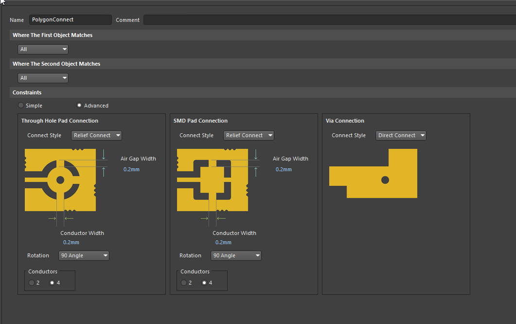
Figure 4: Copper pour rules can separately set the connection methods for through-hole pads, SMD pads, and vias.
About Maxipcb
Maxipcb empowers innovators to turn cutting-edge technologies into reality.We offer one-stop solutions for design, simulation, testing, PCB manufacturing, component procurement and SMT assembly, enabling efficient development, rapid deployment and risk control across the full product lifecycle.
Serving the world in communications, industrial automation, aerospace, automotive, semiconductor and beyond, we build a safer, more connected future together.
