Recently I came across a 2020 blog post by Zachariah Peterson: The Great PCB Layout Rules of Thumb Debate Rages On, which discusses widely debated PCB design rules of thumb.
Recently I came across a 2020 blog post by Zachariah Peterson: The Great PCB Layout Rules of Thumb Debate Rages On, which discusses widely debated PCB design rules of thumb.
Many 20‑year‑old PCB routing rules are still followed today. But are they still valid? The answer is:
it depends.
The debate over rules is not about right or wrong, but about
when and where to apply them. This article clarifies the applicable scenarios for these classic rules.
01 Orthogonal (Vertical) Routing
Orthogonal routing requires traces on adjacent signal layers to be perpendicular to reduce crosstalk from mutual inductance.
At low frequencies (below a few GHz), capacitive coupling between perpendicular traces is low.
In the RF band (dozens of GHz), cavity resonance and ungrounded structures cause strong electromagnetic resonance. Even perpendicular traces can produce severe crosstalk.
The most effective solution is to use ground planes between signal layers for isolation. When in doubt, use crosstalk simulation to verify noise margins. Return path planning is also critical.
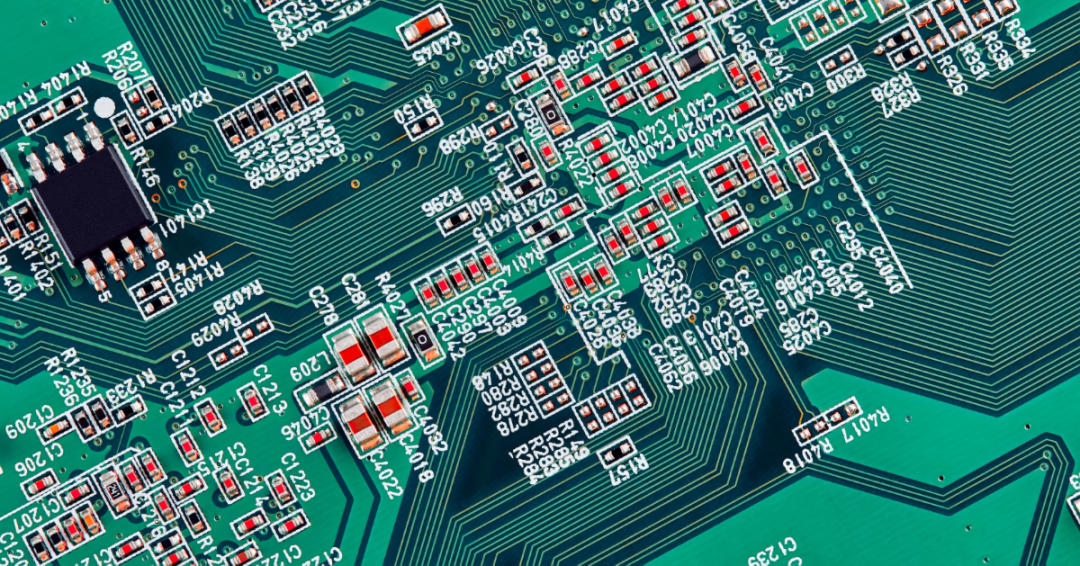
Figure 1.1.1 – Can you find orthogonal routing in this complex PCB?
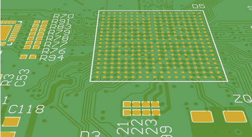
Figure 1.1.2 – True orthogonal routing is nearly impossible in advanced PCB design
02 Thermal Relief Vias
This is a highly debated rule: some designers never use thermal reliefs and have no assembly issues; others insist on using them for every pad connected to a plane.
Both are correct for different scenarios:
- Hand soldering: Higher iron temperature compensates for heat sinking.
- Wave soldering: Thermal reliefs are required to prevent tombstoning, cold joints, and loose components.
Recommendation: Always use thermal reliefs for mass assembly.
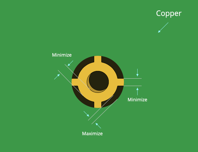
Figure 1.2.1 – Thermal relief solder vias on a ground plane
03 Right‑Angle Routing
Right‑angle routing is the most controversial rule. Many designers still ban 90° bends entirely, using flawed reasoning:
- “Electrons can’t turn right angles” — ignores that vias are vertical.
- “Acid traps in etching” — irrelevant with modern alkaline etching.
- “Impacts impedance” — negligible below 50 GHz (mmWave/5G).
Conclusion: Unless your design operates above 50 GHz, you can safely use right‑angle traces. Modern PCB tools with field solvers make this even easier.
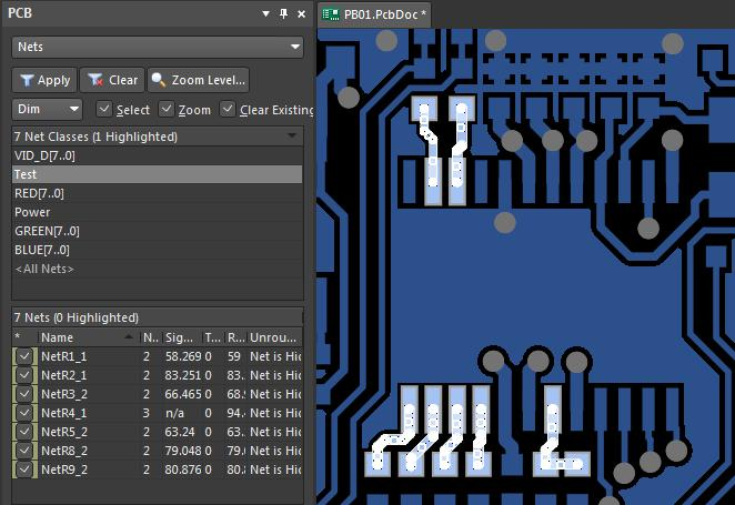
Figure 1.3.1 – Some designers insist all right angles must be chamfered
04 The “3W” Rule
The 3W rule has two versions:
-
Spacing rule: Trace center‑to‑center spacing ≥ 3× trace width to reduce magnetic coupling.
This rule is misleading: EMI depends on
loop overlap area, not just distance. Reduce loop area first.
-
Length‑matching rule: For sawtooth tuning, the notch width ≥ 3× trace width to minimize impedance discontinuity.
Always verify with simulation.
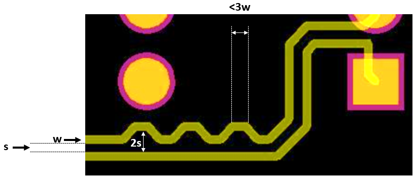
Figure 1.4.1 – 3W rule in sawtooth length‑matching
05 The “20H” Rule
20H means the ground plane overlaps the power plane by 20× the dielectric thickness to suppress edge radiation.
- Effective for reducing emissions below ~300 MHz.
- At high frequencies, the power–ground structure acts like a waveguide, causing resonance and worse interference.
Rule of thumb: Use 20H only if your frequency is below 1 GHz.
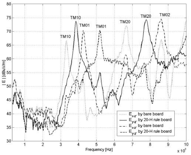
Figure 1.5.1 – RF radiation issues in some 20H‑rule PCBs
About Maxipcb
Maxipcb empowers innovators to turn cutting-edge technologies into reality.
We offer one-stop solutions for design, simulation, testing, PCB manufacturing, component procurement and SMT assembly, enabling efficient development, rapid deployment and risk control across the full product lifecycle.Serving the world in communications, industrial automation, aerospace, automotive, semiconductor and beyond, we build a safer, more connected future together.
