This article covers PCB trace width, trace width calculation, and the relationship between trace width and current.
This article covers PCB trace width, trace width calculation, and the relationship between trace width and current.
1. What is PCB Trace Width?
Trace width is one of the most critical factors in PCB design.
Inexperienced designers often use the default trace width in PCB layout software. For experienced designers, default values are only references; power and ground connections usually require wider traces.
2. What is a Trace?
A PCB trace is a thin conductive copper wire on an insulating substrate, used to transmit signals and power. It has a defined width and thickness.
- Typical copper thickness: 35 µm (1 oz/ft²)
- Minimum manufacturable trace width: 6 mil (0.152 mm)
- Common design width: 0.254–0.3 mm for process tolerance
3. Key Factors Affecting Trace Width
① Signal Traces
Trace width is less critical for low-speed signals, but vital for RF, analog, and high-speed digital designs because trace width and impedance are inversely related.
② Power Traces
Power traces require special attention for two reasons:
-
Current-carrying capacity
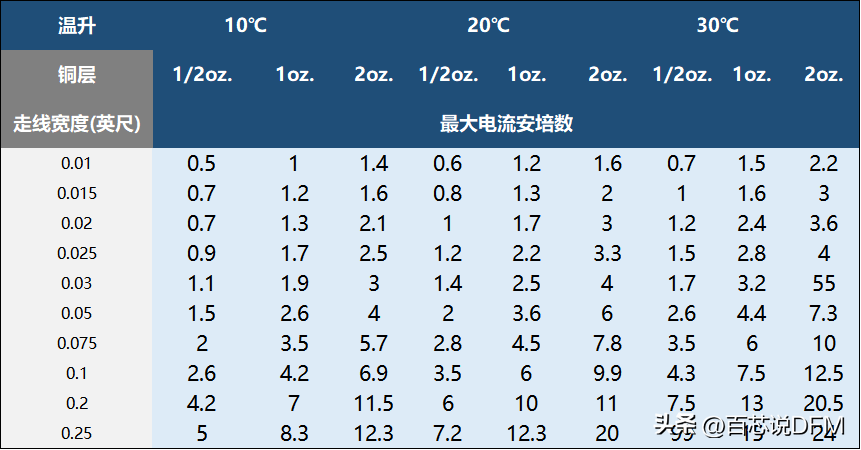
Cross-sectional area (copper thickness × width) determines how much current a trace can carry without overheating.
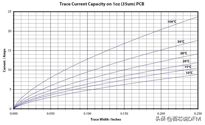
Current-carrying capacity diagram
The
IPC-2152 standard provides empirical data for current vs. temperature rise.
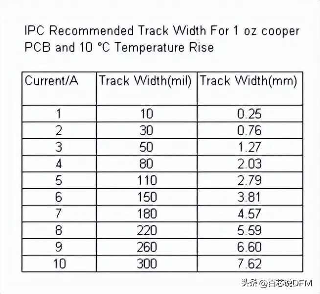
Trace width vs. current for 1 oz copper at 10 °C temperature rise
Online calculators can compute the required width for a rated current and temperature limit. Inner layers often need wider traces due to poorer heat dissipation.
-
Trace impedance
High-speed circuits require controlled impedance to minimize crosstalk, coupling, and reflections. At GHz frequencies, traces act as transmission lines with series inductance, resistance, and parasitic capacitance.
③ Trace Width and Signal Reflection
Signal reflection causes distortion and ringing. A 90° bend increases effective width to ~1.414× the nominal width, changing impedance and causing reflections. Sharp bends and uneven widths should be avoided.
Signal reflection caused by trace width change at bends
Other considerations:
- Component pad size and pitch
- Spacing between traces (prevents short circuits)
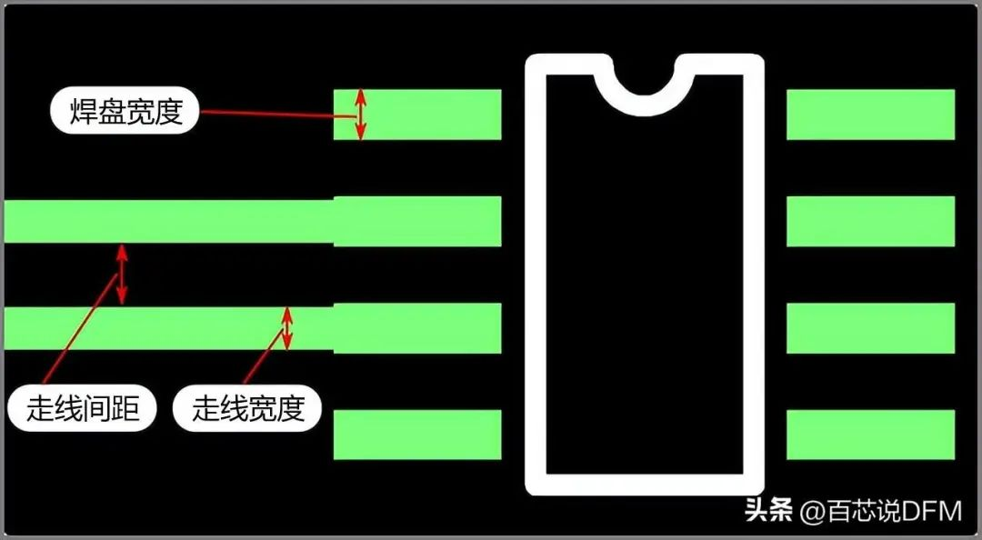
- Trace width illustration
4. How to Calculate PCB Trace Width
① Using a Trace Width Calculator
Input: maximum current, trace length, allowable temperature rise. The calculator outputs the minimum safe width. Inner layers typically need wider traces than outer layers.
② Using Formulas (IPC-2221)
Core formula for allowable current:
I = k × ΔT⁰·⁴⁴ × A⁰·⁷²⁵
- I = current (A)
- ΔT = temperature rise (°C)
- A = cross-sectional area (mil²)
- k = 0.048 (for external traces)
Derive width:
Area = ( I / (k × ΔT⁰·⁴⁴) )^(1/0.725)
Width (mil) = Area / (Thickness (oz) × 1.378 mil/oz)Valid range: 0–35 A, 10–100 °C rise, 0.5–3 oz copper.
Example: 2 A → ~30 mil width for 1 oz copper.
PCB trace width lookup table
5. How to Calculate PCB Trace Resistance
Trace resistance depends on copper resistivity, temperature coefficient, thickness, width, length, and operating temperature. It affects voltage drop in power paths.
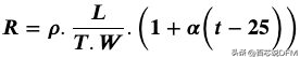
Trace resistance formula and parameters
Practical Example: DC Motor Power Path
A 2 A motor supply trace (0.8 inches long, 1 oz copper) requires calculating minimum width and voltage drop.
Optimized trace width for DC motor power path
6. Role of Trace Width in PCB Layout
① Signal Integrity
- Controls interference, crosstalk, and EMI
- Controlled impedance routing for high-speed signals
- Microstrip / Stripline for shielding
② Analog Routing
Use short, direct, wide traces; minimize vias.
③ Power Integrity
- Short, direct paths; rounded corners
- Wide traces to reduce inductance and crosstalk
- Thermal management (outer layers benefit from air cooling)
Example 1: High-Speed USB Routing
USB 2.0 High Speed needs
90 Ω differential impedance, matched length (<50 mil mismatch), optimized width and spacing.

USB 2.0 High-Speed differential routing
Example 2: DDR3 Routing
Requires tight length matching; tools automate length tuning.

DDR3 layout with length-tuned traces
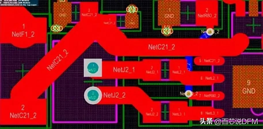
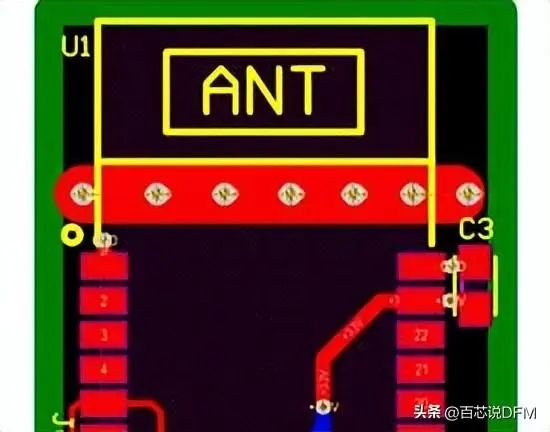
Example 3: Ground Vias for Noise Suppression
Embed ground vias around sensitive circuits (e.g., Bluetooth, antennas) to reduce coupling.
Bluetooth module with grounded via traces for isolation
Ground plane with vias on sensitive PCB perimeter
7. Typical Trace Widths and Thicknesses
- Thin traces: General TTL signals
- Thick traces: High-power peripherals (motors, fans)
- Differential pairs: USB, high-speed signals (controlled impedance)
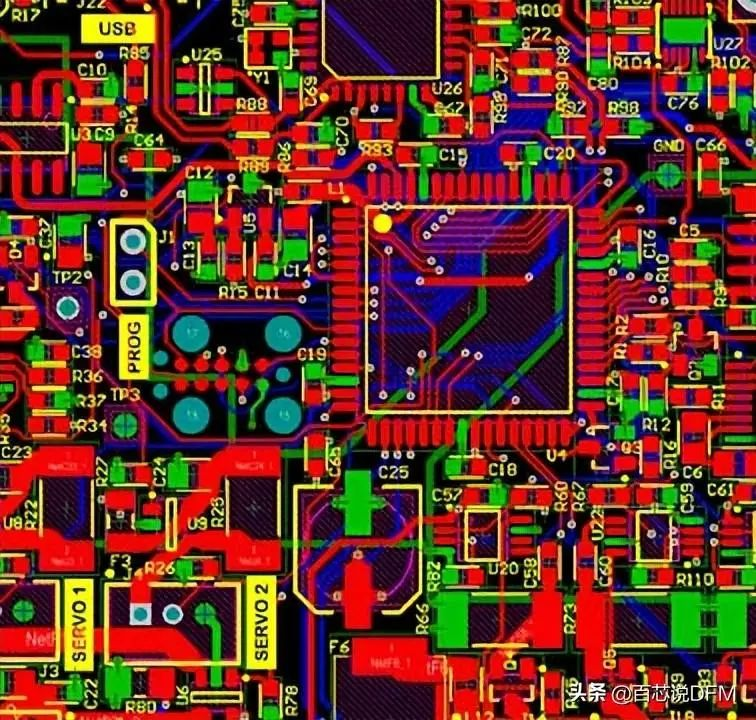
Example 4-layer board with mixed trace widths

Example 6-layer board with 5 mil traces for 256-pin BGA
8. PCB Manufacturing Specifications
These features increase manufacturing cost:
- Trace width < 5 mil
- Trace spacing < 5 mil
- Via diameter < 8 mil
- Copper thickness < 1 oz or > 1 oz
- Controlled impedance / differential pairs
- High-density layouts (fine-pitch BGA)
High-voltage designs require extra spacing to prevent arcing.
About Maxipcb
Maxipcb empowers innovators to turn cutting-edge technologies into reality.
We offer one-stop solutions for design, simulation, testing, PCB manufacturing, component procurement and SMT assembly, enabling efficient development, rapid deployment and risk control across the full product lifecycle.Serving the world in communications, industrial automation, aerospace, automotive, semiconductor and beyond, we build a safer, more connected future together.


