
Pouring ground copper into blank PCB areas is very common, but when copper pour is close to high-speed or RF traces, it may directly change impedance and field distribution. This article explains from three perspectives—microstrip, coplanar structure, and spacing—when copper should be poured and when distance should be kept.
When PCB layout is nearing completion, many engineers do the same thing: pour as much of the blank area as possible as GND.
The reasoning is also intuitive—more ground copper looks like better return paths, stronger shielding, and lower EMI.
But for high-speed signals and RF traces, the copper beside traces is not better the more there is. If the distance is wrong, it can directly change the impedance you originally calculated.
You Originally Calculated a Microstrip, but After Copper Pour It May Have Become Another Structure
For many controlled-impedance traces, the default structure during calculation is microstrip: one signal trace on the top layer and a complete reference ground plane below.
In this case, impedance is mainly determined by trace width, copper thickness, dielectric thickness, and dielectric constant.
But if you also pour ground copper on the left and right sides of the signal trace, and the distance is very close, the electric field no longer travels only toward the reference plane below; it also couples to the ground copper on both sides.
At this point, the structure begins to approach a grounded coplanar waveguide, commonly called coplanar waveguide with ground.
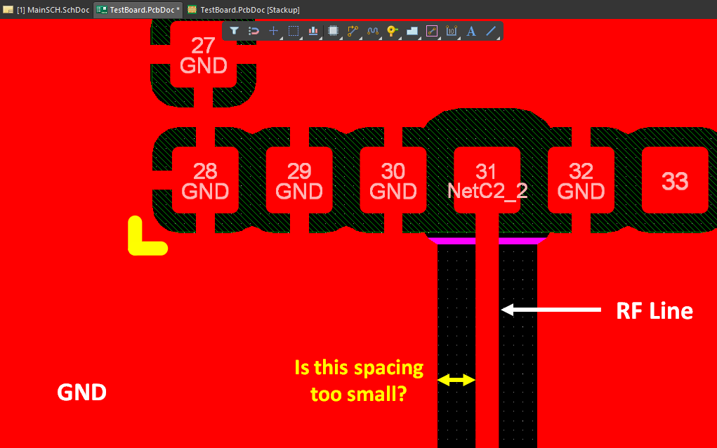 Figure 1: For a trace originally designed as an ordinary microstrip, if the ground copper on both sides is very close, the actual electromagnetic field distribution will change.
Why Does Impedance Decrease?
You do not need to memorize complex formulas first; just remember an intuitive conclusion: the closer the ground copper beside the trace, the stronger the coupling between the signal trace and ground usually is.
After coupling increases, the capacitance per unit length increases, and the characteristic impedance changes accordingly.
Therefore, an RF trace originally calculated as a 50 Ω microstrip may very likely no longer be the original 50 Ω if, after layout is completed, GND copper pour is suddenly placed very close on both sides.
This is also why a true coplanar structure requires bringing the trace width W and the gaps on both sides into the impedance calculation together, rather than calculating only the trace width.
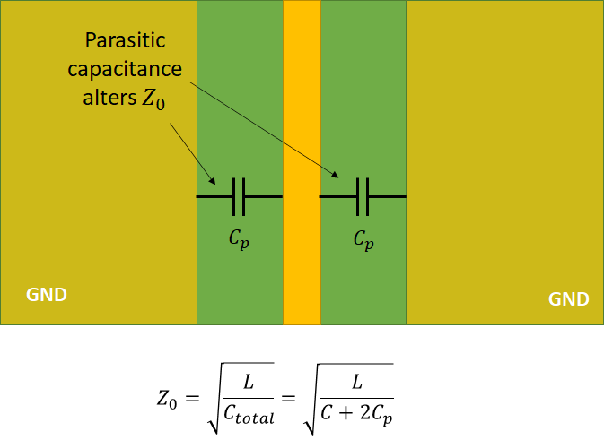 Figure 2: The spacing between the surface ground copper and the signal trace participates in impedance formation. The smaller the spacing, the more obvious the impact on the original trace parameters usually is.
So Should No Copper Be Poured Beside High-Speed Lines? Not Exactly.
If you designed according to a coplanar structure from the beginning, then the ground copper on both sides is not a problem; rather, it is part of the design.
RF traces, antenna feed lines, and some high-speed interfaces may all use this structure.
The key is: you need to know whether you are designing a microstrip or a coplanar structure.
The most feared situation is calculating impedance as a microstrip, but in the final layout step casually pouring copper beside the trace—the two sides are using two different sets of assumptions.
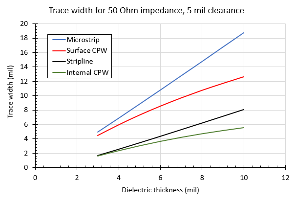 Figure 3: Under the same stack-up, even if the target impedance is the same, the required trace width and spacing may differ between a microstrip and a coplanar structure.
What Should Be Noted When Pouring Copper Beside Ordinary Digital Lines?
For low-speed GPIO and ordinary control lines, pouring ground nearby is usually not as sensitive as with RF traces.
But for high-speed networks such as fast clocks, USB, DDR, and PCIe, the nearby copper pour should be treated as part of the transmission-line geometry.
In particular, avoid a situation where one section of copper is very close and another section suddenly retreats far away.
Because this geometric change causes local impedance changes, equivalent to artificially adding a discontinuity in the line.
Via Stitching Is Not “the More You Place, the More Professional It Is”
If the surface copper pour is just a large floating area but has poor connection to the actual GND reference plane, it may not provide the shielding effect you imagine.
A coplanar ground structure usually needs to connect the surface ground to the reference plane below through reasonable ground vias.
But ground via spacing should also be planned according to the highest operating frequency and structure dimensions, rather than mechanically placing a ring every few millimeters.
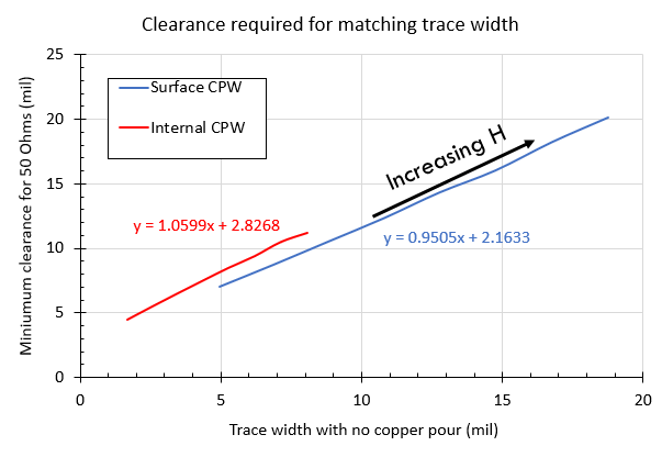 Figure 4: Ground copper and ground vias near high-speed or RF traces should be considered together as a complete structure, avoiding floating or insufficiently connected copper areas.
During Actual Design, Ask Yourself 3 Questions First
Does this line need impedance control? If so, what transmission-line structure did I use in the calculation? After layout is completed, has the actual structure of the surrounding copper pour and reference plane changed?
If these 3 questions can be matched up, copper pouring usually will not become a “casual final-step operation.”
For important high-speed channels, you can also use impedance calculation tools, field solvers, or after the board is fabricated use TDR or VNA to verify.
Copper pouring itself is not the goal. For high-speed signals, what truly matters is keeping the geometric structure of the entire transmission line controllable and continuous, rather than filling every blank area with copper.