I. Layout Precautions
(1) Structural Design Requirements
It is necessary to clarify the product structure before PCB layout.
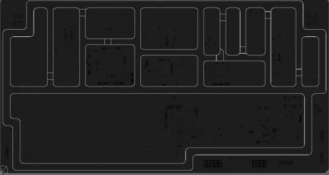
The structure needs to be reflected on the PCB board. For example, the outer edge thickness of the cavity shell, the thickness of the middle partition cavity, the chamfer radius, and the screw size on the partition cavity (in other words, the structural design is carried out according to the outline (structural part) drawn on the completed PCB). Generally, the outer cavity thickness is 4mm; the inner cavity width is 3mm; for dispensing process, it is 2mm; the chamfer radius is 2.5mm. Taking the lower left corner of the PCB board as the origin, the partition cavity must be an integer multiple of the grid 0.5, and at least an integer multiple of the grid 0.1. This is conducive to processing by structural processors and more accurate error control. Of course, this needs to be designed according to customer requirements.
Figure 1 - Structural outline diagram on PCB
(2) Layout Requirements
Prioritize the layout of the RF link, then layout other circuits.
A. Precautions for RF Link Layout
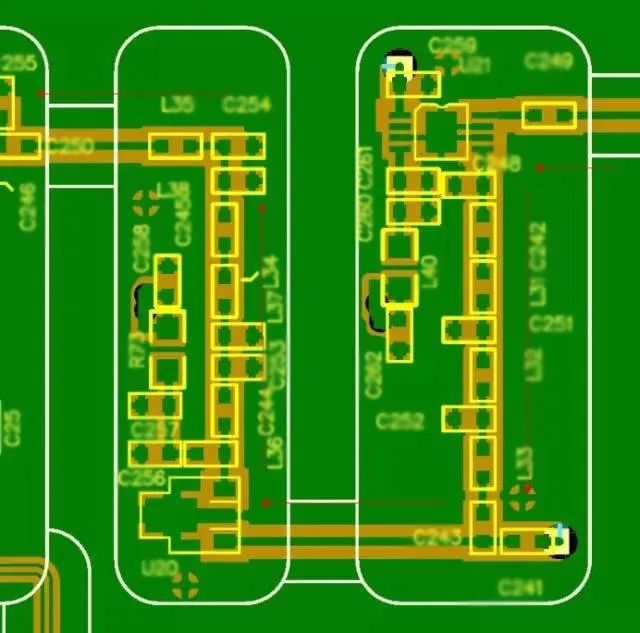
Layout completely according to the sequence of the schematic diagram (from input to output, including the sequential position of each component and the spacing between components. Some components should not be too far apart, such as π networks). Layout in a "straight line" or "L" shape. In actual RF link layout, due to product space constraints, it may not be fully realized, which forces us to layout in a "U" shape. U-shaped layout is not impossible, but a partition cavity needs to be added in the middle to isolate the left and right sides for good shielding.
Figure 2 - U-shaped layout with partition cavity
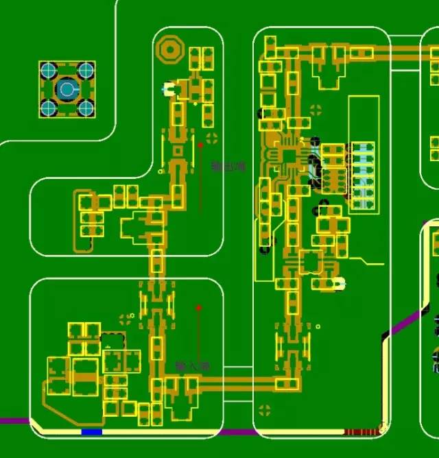
There is also a case where a partition cavity needs to be added horizontally. That is, use a partition cavity to isolate the left and right sides of the straight line. This is mainly because the part to be isolated is very sensitive or easy to interfere with other circuits; in addition, it may also be because the gain of the circuit from the input end to the output end of the straight line is too large, which also needs to be separated by a partition cavity (if the gain is too large and the cavity is too large, it may cause self-excitation).
Figure 3 - Straight line layout with partition cavity
B. Peripheral Circuit Layout of Chips
The peripheral circuit layout of RF devices shall be strictly in accordance with the requirements on the datasheet, and can be adjusted if limited by space; the peripheral circuit layout of digital chips will not be elaborated here.
II. Routing Precautions
Route according to the 50-ohm impedance line width, try to exit from the center of the pad, keep the line straight, and route on the surface layer as much as possible. Make 45-degree or arc turns where turning is required, and it is recommended to turn on both sides of capacitors or resistors. If there are device routing matching requirements, route strictly according to the reference length on the datasheet. For example, the required routing length between an amplifier tube and a capacitor (or between inductors), etc.
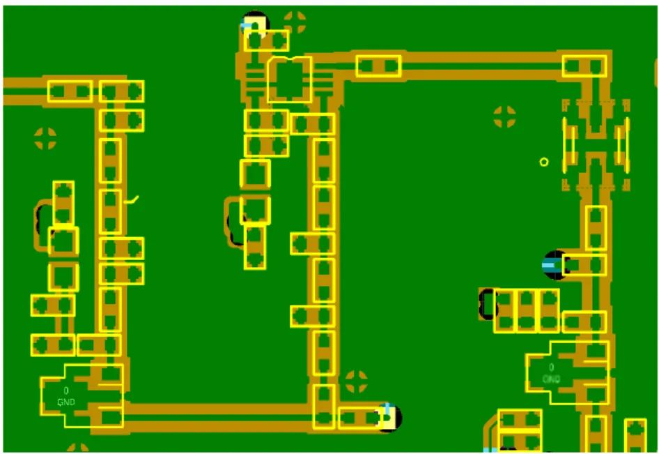
Figure 4 - Using device pads as turning points
In PCB design, to make the high-frequency circuit board design more reasonable and have better anti-interference performance, the following aspects should be considered (general practices):
(1) Reasonable Selection of the Number of Layers
When routing high-frequency circuit boards in PCB design, using the middle inner layers as power and ground layers can play a shielding role, effectively reducing parasitic inductance, shortening signal line lengths, and reducing cross-interference between signals.
(2) Routing Method
Routing must turn at 45-degree angles or arcs, which can reduce the emission of high-frequency signals and mutual coupling between them.
(3) Routing Length
The shorter the routing length, the better, and the shorter the parallel distance between two lines, the better.
(4) Number of Vias
The fewer the number of vias, the better.
(5) Inter-layer Routing Direction
The inter-layer routing direction should be vertical, that is, the top layer is horizontal and the bottom layer is vertical, which can reduce interference between signals.
(6) Copper Pouring
Increasing grounded copper pouring can reduce interference between signals.
(7) Ground Wrapping
Ground wrapping important signal lines can significantly improve the anti-interference ability of the signal. Of course, ground wrapping can also be performed on interference sources to prevent them from interfering with other signals.
(8) Signal Lines
Signal routing cannot form loops and needs to be routed in a daisy-chain manner.
III. Grounding Treatment
(1) RF Link Grounding
The RF part adopts a multi-point grounding method for grounding treatment. The copper pouring gap of the RF link is generally 30mil to 40mil, which is more commonly used. Grounding holes need to be drilled on both sides, and the spacing should be kept as consistent as possible. For the grounding pads of capacitors and resistors to ground on the RF path, drill grounding holes as close as possible. All grounding pads on the device need to be drilled with grounding vias.
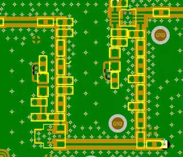
Figure 5 - Grounding holes in RF path
(2) Cavity Shell Grounding Holes
To achieve better contact between the cavity shell and the PCB board, generally two rows of grounding holes are drilled and placed in a staggered manner, as shown in Figure 06. Windows need to be opened on the PCB partition cavity, as shown in Figure 07. All places where the bottom layer grounding copper of the PCB contacts the bottom plate need to be windowed for better contact, as shown in Figure 08 (the upper part of the PCB board contacts the base):
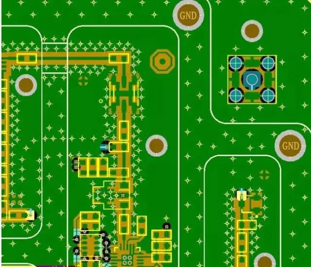
Figure 6 - Grounding vias on PCB partition cavity
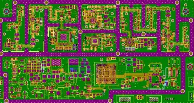
Figure 7 - Windowing on PCB partition cavity
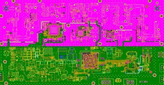
Figure 8 - Windowing on PCB bottom layer
(3) Screw Placement (Requires Knowledge of Structure)
To achieve tighter contact between the PCB and the base and cavity shell (better shielding), screw hole positions need to be placed on the PCB board.
Screw placement method between PCB and cavity shell: Place a screw at each intersection of the partition cavities. In actual design, it is difficult to achieve, and can be appropriately adjusted according to the module circuit function. However, in any case, there must be screws at the four corners of the cavity shell.
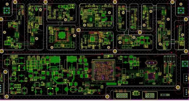
Figure 9 - Cavity shell screws
Screw placement method between PCB and base: Screws are required in each small cavity in the cavity shell, and the number of screws depends on the cavity size (the larger the cavity, the more screws are placed). The general principle is to place screws at the opposite corners of the cavity. Screws must be placed next to SMA connectors or other connectors to prevent PCB board deformation during plugging and unplugging of SMA connectors or connectors.
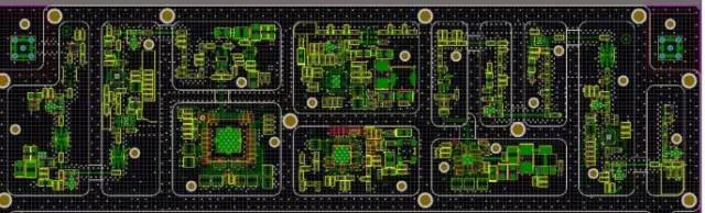
Figure 10 - Screws in the cavity
About Maxipcb
Maxipcb empowers innovators to turn cutting-edge technologies into reality.
We offer one-stop solutions for design, simulation, testing, PCB manufacturing, component procurement and SMT assembly, enabling efficient development, rapid deployment and risk control across the full product lifecycle.Serving the world in communications, industrial automation, aerospace, automotive, semiconductor and beyond, we build a safer, more connected future together.