PCB is widely used in our life now, so there is an increasing demand for the reliability of products. In view of this demand, it is necessary to introduce simulation methods to improve the quality of our products, and identify the corresponding problems through simulation at the initial stage of design, so as to deal with them in a targeted manner.
1. Introduction
PCB is widely used in our life now, so there is an increasing demand for the reliability of products. In view of this demand, it is necessary to introduce simulation methods to improve the quality of our products, and identify the corresponding problems through simulation at the initial stage of design, so as to deal with them in a targeted manner.
In our early technical articles, we elaborated in detail how to quickly realize the modeling and accurate simulation analysis of complex chips or PCB models through the function of trace mapping (the next article). This article will further provide new methods to achieve more accurate analysis on the basis of the original.
First of all, let's review the previous problems about PCB reliability. PCB has different working conditions such as temperature change, cutting and vibration during manufacturing and actual use. How to ensure that the related defects can be quickly analyzed and solved in similar environment, there are two key factors, namely modeling and material parameters.
Modeling It is very difficult to completely model this kind of products in finite element because of the size specification of PCB or chip, so in the last article, we provided trace mapping function, which can conveniently and efficiently model the structure of PCB and accurately define the material properties of each layer of PCB, so it can quickly analyze complex PCB products.
2.Reinforcement
Trace mapping is based on the mapping function of metal volume fraction to reflect the material information of the stack and via hole in PCB, and the result only reflects the deformation and stress of the corresponding model structure on this basis. However, when we need to locate the defect position in detail or check the detailed deformation of the stack, this function cannot meet our requirements, so we need to introduce another function.
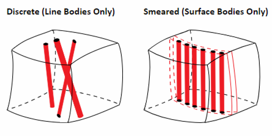
For properly modeled geometry, Mechanical provides the option of specifying Reinforcement materials within the structure. Mechanical can use special enhancement components to model these enhanced geometries. These enhancement elements provide additional enhancements by interacting with standard structures or hot spots through shared nodes. As shown in the figure, Mechanical provides reinforcement specifications for line bodies (discrete reinforcement materials) and surface bodies (dispersion reinforcement materials). Each wire designated as a reinforcing material basically represents reinforcing fibers with arbitrary orientation in space. Each surface body designated as a reinforcing material basically represents a reinforcing layer. The reinforcement layer can be a homogeneous reinforcement layer or a reinforcement layer with uniformly spaced fibers.
3. Sherlock
How to add compensation needs another Ansys software, Sherlock. Sherlock is a software for life prediction and analysis of PCB based on failure physical model, and it is currently one of the few automatic design reliability analysis software based on POF in the world. Its principle is based on the actual physical process of product failure, through the construction of the corresponding mathematical model, to achieve the purpose of quantitative description and evaluation of product failure, and then to assist in the completion of product design optimization, product reliability growth and protection and other product research and development purposes.
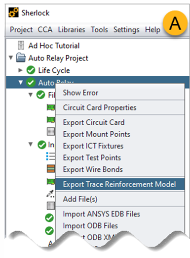
In addition to analyzing the life of PCB, Sherlock has a special function. It can generate the laminated model of each layer of PCB, import the laminated output into the Mechanical model, model the laminated and via holes as reinforcing components in the Mechanical model, and open the exported model in the Workbench Mechanical. The following properties will be automatically applied according to the settings in Sherlock: the thickness of the trace model, the shell compensation element, the through-hole cross section of the beam compensation element, and all corresponding material properties. The flow chart is as follows:
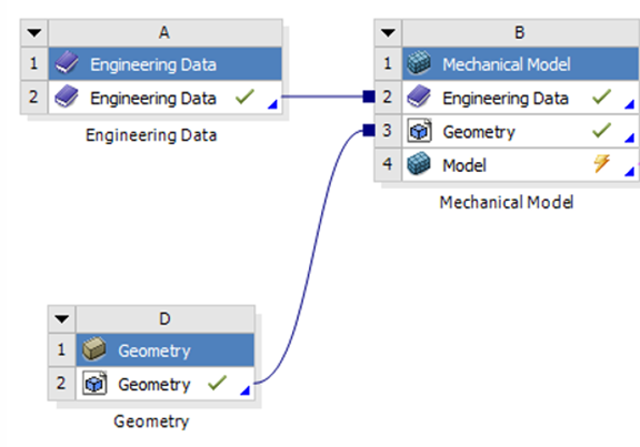
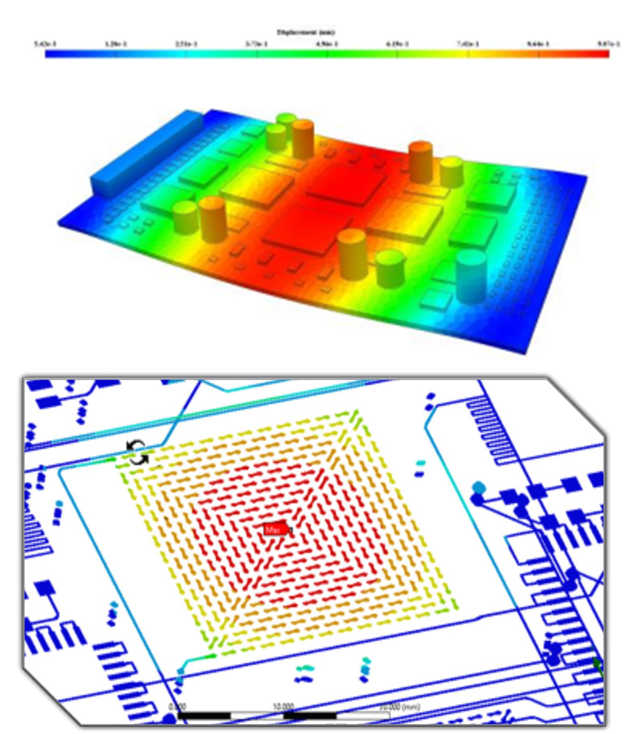
Combine the output stack with the PCB model, and set the feedback unit for the imported stack model. After combining the two, we can get more detailed analysis results. On this basis, we can better check the stress and deformation of related stacks, as shown in the figure:
4. Conclusion
Combined with the stacking function of Sherlock and trace mapping, the PCB model can be accurately modeled and more detailed results can be obtained.
About Maxipcb
Maxipcb empowers innovators to turn cutting-edge technologies into reality.
We offer one-stop solutions for design, simulation, testing, PCB manufacturing, component procurement and SMT assembly, enabling efficient development, rapid deployment and risk control across the full product lifecycle.
Serving the world in communications, industrial automation, aerospace, automotive, semiconductor and beyond, we build a safer, more connected future together.

