A product adopts a frame backplane structure, and other PCB boards are inserted on the backplane and interconnected through the backplane. The backplane PCB is installed on the front backplane, and other PCB boards are vertically connected with the backplane.
[Description of phenomenon]
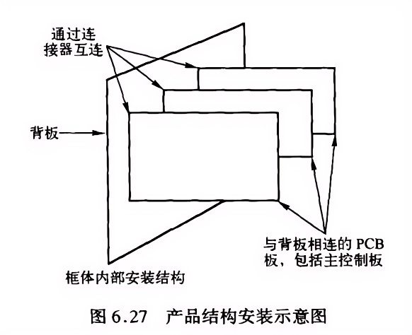
A product adopts a frame backplane structure, and other PCB boards are inserted on the backplane and interconnected through the backplane. The backplane PCB is installed on the front backplane, and other PCB boards are vertically connected with the backplane. The schematic diagram of product structure installation is shown in Figure 6.27. The frame is powered by -48V DC. The -48V power signal is transmitted to each PCB board inserted in the frame and connected to the backplane through the backplane. Among them, the main control panel is the general control system of the frame system.
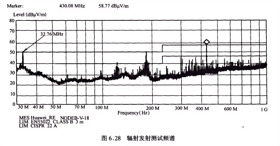
During the radiation emission test, it is found that the radiation is high at the frequency point of 32.76MHz, and the quasi-peak value is 53.8dBμV/m, which exceeds the CLASS A limit by nearly 4 dB, as shown in Figure 6.28.
In the process of positioning, it is found that the main control board disappears when it is not inserted in the slot. As long as the main control board is inserted, the radiation at this point exists no matter how other PCB boards are configured. During the positioning process, it is also found that if a magnetic ring is connected to the power line, the radiation at this point will also disappear, which means that this point radiates through the power line, and the source of this frequency point comes from the main control board, and the coupling path may be on the main control board or the backplane.
[Cause analysis]
In order to determine the coupling path of the radiation source, firstly, the back plate of the frame and the PCB of the main control board are inspected in detail.
By checking the PCB wiring of the backplane and the main control board, it is found that there are several possible ways and reasons for the interference signal to couple to the power line:
(1) The clock trace in the slot of the main control panel on the backplane is close to the -48V ground of the power supply of the frame, and the isolation distance from the backplane DGND is 50mil, which may be coupled to the power supply line.
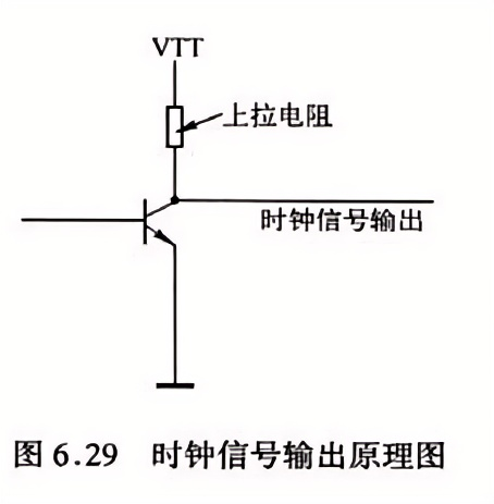
(2) The routing of the clock line is matched at both ends and matched to the VTT power layer through the pull-up resistor. The schematic diagram of clock signal output is shown in Figure 6.29.
If the VTT filter capacitor is not properly selected, the interference may be transmitted to the VTT layer, and the VTT layer and the -48V power supply layer have a large area overlap on the main control board, and the -48V power supply layer is likely to be coupled to the interference.
After the above preliminary analysis, the positioning test can be carried out according to the following steps:
Step one
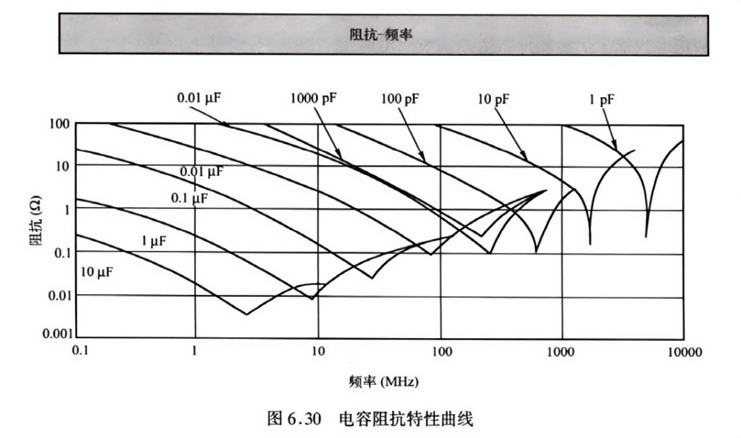
The filter capacitance of the clock matching resistor of the back plate of the frame is optimized to be 0.1μF and 0.022 μ f..
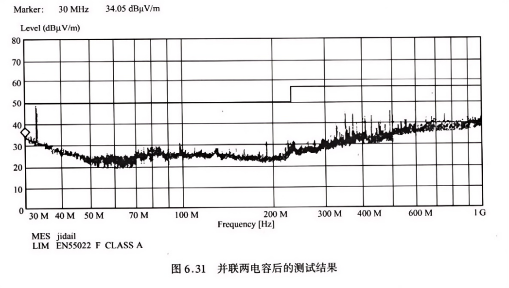
From the capacitance impedance characteristic curve shown in Figure 6.30, it can be seen that the filtering range of two capacitors in parallel is between tens of MHz. After modification, the test is carried out again, and the test result after two capacitors are connected in parallel is shown in Figure 6.31.
The test results in Figure 6.31 are improved compared with the previous test results, indicating that the interference is related to the VIT power layer, but the coupling occurs in the backplane or the main control board, which needs further positioning.
Step 2
Pull up the 32.768MHz clock output by the main control board to VTT by using specially processed connectors, and then start the main control board. The schematic diagram of pulling up through the connectors is shown in Figure 6.32.
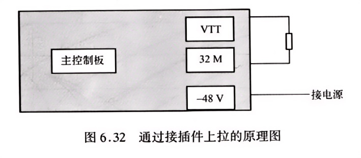
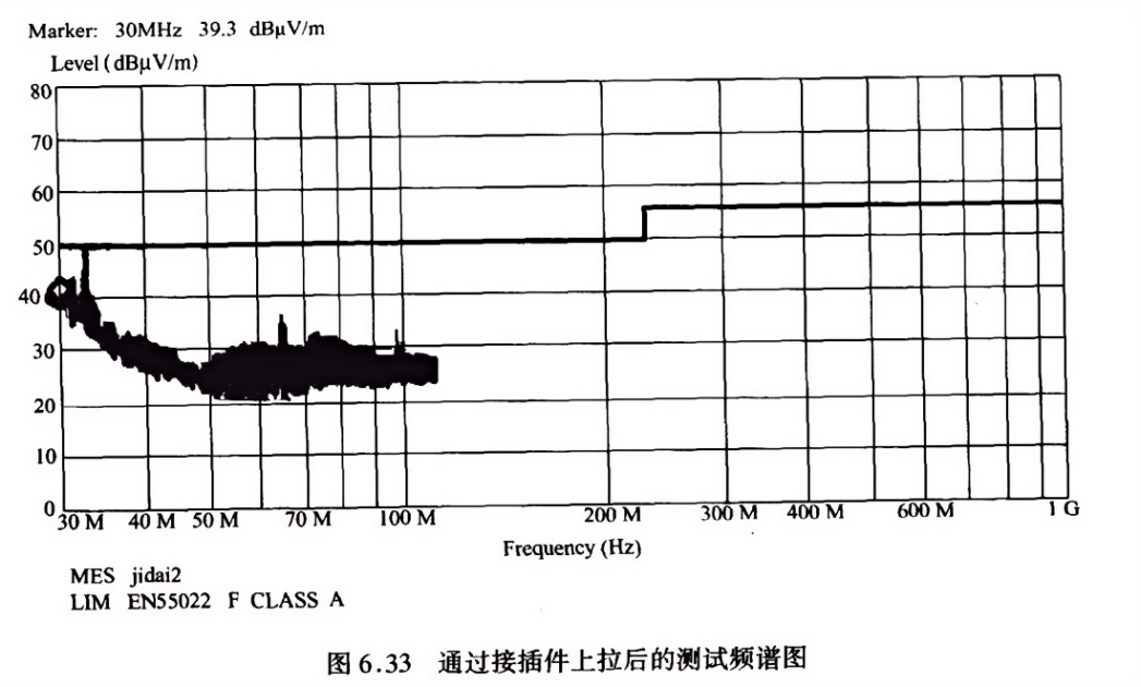
After the connector is pulled up, it is tested, and the result is shown in Figure 6.33.
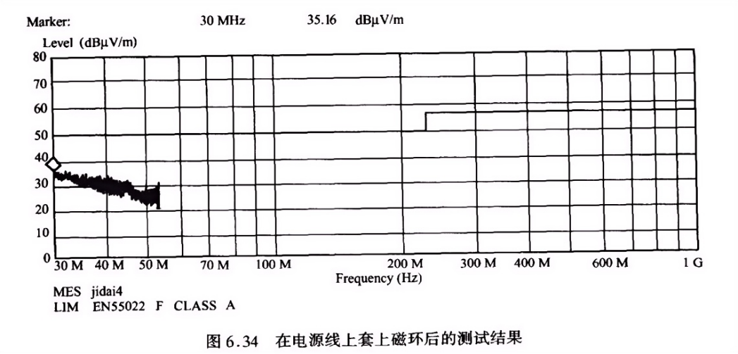
Then put a magnetic ring on the power cord and test it, and get the result as shown in Figure 6.34.
So far, it can basically be explained that the problem lies in the main control board, not the backplane, but the coupling inside the main control board. What needs to be further located is whether the coupling is caused directly by the clock line or by the VTT power layer.
Step 3
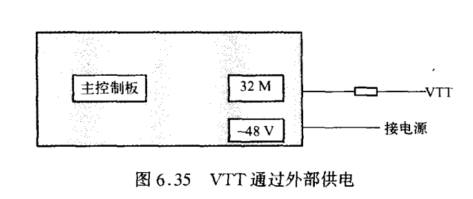
Deal with the main control panel, and turn off the VTT power supply of the main control panel. The VTT is powered by an external linear power supply and then connected, as shown in Figure 6.35.
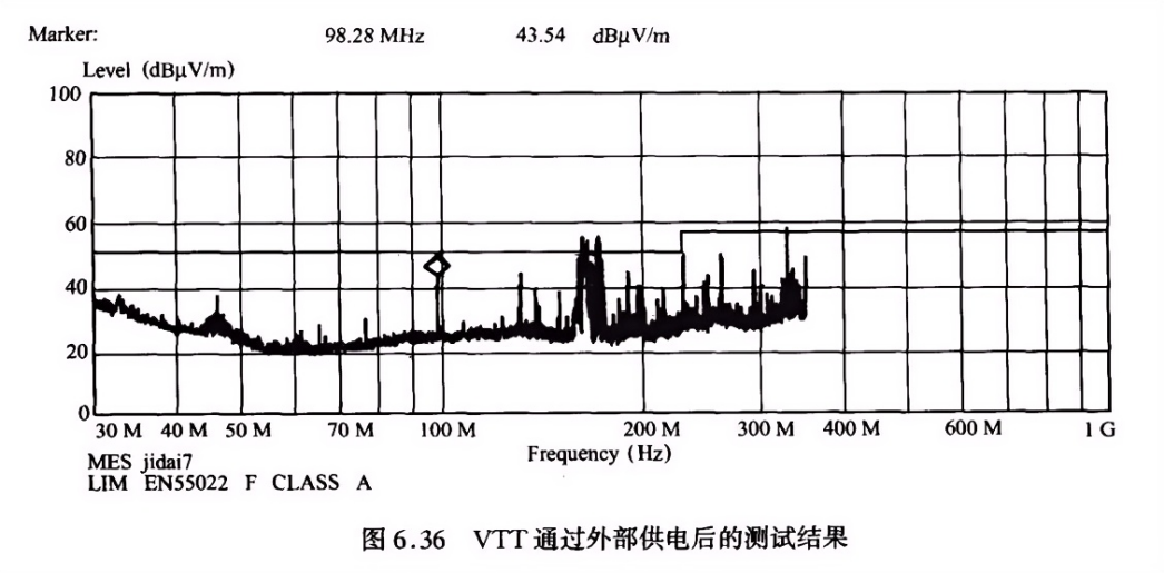
After starting the main control panel, conduct radiation test, and get the result as shown in Figure 6.36.
The 32.768 MHz clock radiation basically disappeared, indicating that the radiation exceeded the standard not because the clock line was directly coupled to the -48V power supply layer, but because the VTT power supply layer of the clock signal was coupled to the -48V power supply layer after being affected by the clock signal.
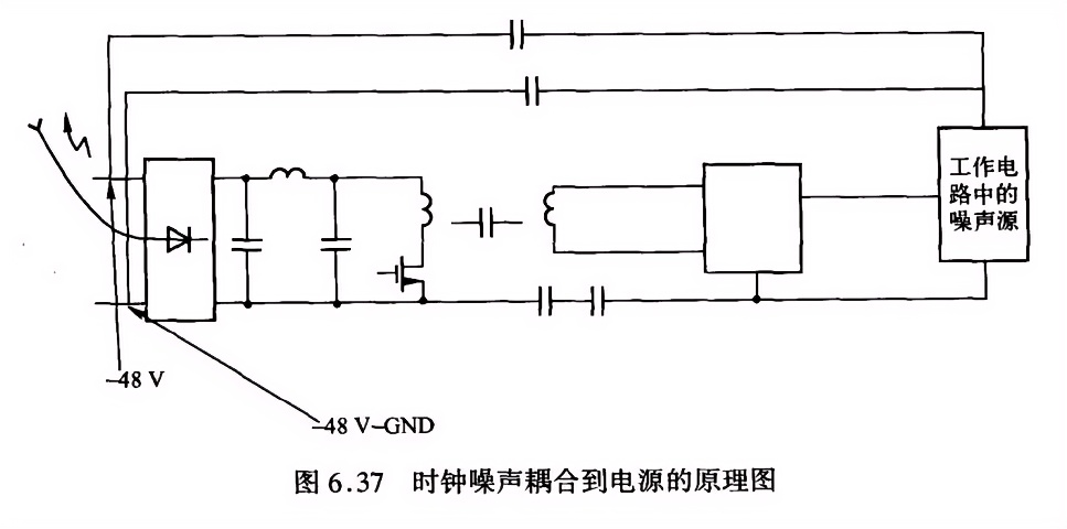
The test shows that the radiation of 32.768 MHz clock is coupled to the -48V power supply layer in the main control board through VTT, and then the main control board is examined. It is found that the power supply layer of VTT overlaps with the power supply planes of -48V and -48-GND in a large area, so that the clock noise in VTT is coupled to the lines of -48V and -48-GND through capacitive coupling. The schematic diagram of clock noise coupled to power supply is shown in Figure 6.37.
[Measures]
(1) Change the power plane distribution of the power layer VTT of the main control panel to avoid the -48V power plane, so that the area where the -48V power plane is located has no other planes except the -48V power and its ground plane.
(2) Optimize the decoupling capacitance of VTT power supply to 0.1μF and 0.022 μ f..
[Thinking and Enlightenment]
(1) PCB population power supply and its related circuits should be well isolated and decoupled from other circuits in PCB, so that the power signal is relatively independent, so as to avoid the signal in PCB merging into the power signal.
(2) For isolated power supply, it is necessary to isolate both the level line and the "0V" line.
About Maxipcb
Maxipcb empowers innovators to turn cutting-edge technologies into reality.
We offer one-stop solutions for design, simulation, testing, PCB manufacturing, component procurement and SMT assembly, enabling efficient development, rapid deployment and risk control across the full product lifecycle.
Serving the world in communications, industrial automation, aerospace, automotive, semiconductor and beyond, we build a safer, more connected future together.


