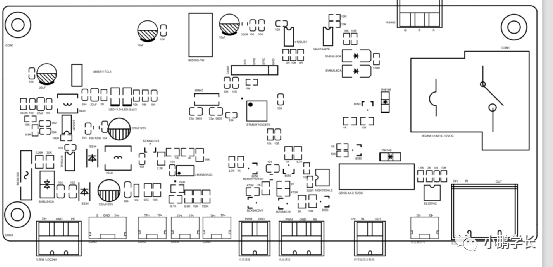
This article is a practical PCB design and layout guide for engineers, covering component placement, routing, copper pouring, soldering files, structure, and DRC check.
This article is a practical PCB design and layout guide for engineers, covering component placement, routing, copper pouring, soldering files, structure, and DRC check.
1. Component Placement
- Align parallel components using alignment tools in AD20.
- For multilayer boards, change Signal layers to Plane layers in the Layer Stack Manager.
- Keep 3 mm clearance between through‑hole and SMD components.
Capacitor Placement
- Align electrolytic capacitor negatives in the same direction (all up or all down).
- Text height: 0.9 mm, width: 0.1 mm.
- Place large capacitors first, small capacitors behind them.
Power Layout
- DC‑DC (high current): Place near the power input.
- LDO (low current): Place near the load.
- Use T+S in the schematic to select components; use I+L to auto‑place them in a region.
- Combine connectors that need mutual fixation into one footprint.
- Use Alt + mouse to highlight ratsnest lines and check layout rationality.
2. PCB Routing
- Route top layer mostly horizontally, bottom layer vertically (or vice versa).
- Low‑frequency signals: can use vias.
- High‑frequency signals & crystal: avoid vias.
- Do not route high‑frequency signals across chips.
- Route signals on the top layer first; use solid copper for power/ground.
- Route signals of the same module in groups.
- High‑impedance input traces: short and wide.
- Power pins of chips: use sufficiently wide traces.
- Avoid acute angles connecting components; keep clearances wide.
- Isolate high‑voltage and low‑voltage circuits (slot or 10 mm clearance).
- Isolate high‑voltage sensing lines from signal lines.
- Crystal traces: length‑matched.
- Power traces: no loops (prevent eddy currents); use multiple vias for conduction.
- Plan power path, voltage, current, via size, trace width, and spacing early.
- Set net colors: PCB → Classes → right‑click → last option.
- Route critical signals first; keep parallel and length‑matched; avoid crossing plane splits.
- Single‑point grounding: merge input and output GND at the IC GND.
- Do not mix Tx/Rx networks.
- Too many crossovers? Place components on the bottom or use vias.
- Do not route traces through magnetics (inductors, transformers).
- Current capacity: 1 mm width ≈ 2 A for 1 oz copper.
- BGA: perform fanout routing; ball pitch = center‑to‑center distance.
- Differential pairs: use Differential Pairs Editor → Create From Nets → Wizard.
3. Copper Pouring
- Classify circuits: input, output, isolated, high‑voltage, high‑power.
- No copper on isolated channels, high‑voltage, or high‑power sections.
- Pour GND copper; enable remove dead copper.
- Add ground vias neatly (aligned); avoid copper islands.
- Clearance rule: 20 mil; connect copper directly.
- Use polygon cutouts to exclude copper from specific areas.
- No copper at screw mounting holes.
4. PCB Soldering Documentation
- Use Smart PDF to export assembly drawings.
- Text height: 0.9 mm, font: TrueType.
- Top layer: check Top Overlayer + Keep‑Out Layer.
- Bottom layer: check Bottom Overlayer + Keep‑Out Layer + Mirror.
5. PCB Structure
- Solder mask opening: for heat dissipation and high‑current areas (use Solder layer).
- Holes: for screws/standoffs (draw circle on Keep‑Out Layer → Board Cutout).
- Batch vias: use stitching vias / shielding vias.
- Via rules: Plane → Connection → Advanced → set to direct connect.
- Panelization:
- Matrix panels: use V‑CUT.
- Irregular panels: use stamp holes.
6. Final PCB Check
- Run DRC (Design Rule Check); zero violations required.
- Current capacity reminder: 1 mm trace width = 2 A (1 oz copper).
7. PCB Prototype Order Flow
- Apply for a part number.
- Generate production files (Gerber + drill files).
- Submit non‑order procurement application.
About Maxipcb
Maxipcb empowers innovators to turn cutting-edge technologies into reality.
We offer one-stop solutions for design, simulation, testing, PCB manufacturing, component procurement and SMT assembly, enabling efficient development, rapid deployment and risk control across the full product lifecycle.Serving the world in communications, industrial automation, aerospace, automotive, semiconductor and beyond, we build a safer, more connected future together.