Switching power supplies are widely used due to high efficiency, wide adjustable output voltage, low loss, small size and light weight. However, their stable DC output is often accompanied by an AC component called voltage ripple. Excessive ripple shortens service life and causes noise, so it must be controlled within acceptable limits.
Switching power supplies are widely used due to high efficiency, wide adjustable output voltage, low loss, small size and light weight. However, their stable DC output is often accompanied by an AC component called voltage ripple. Excessive ripple shortens service life and causes noise, so it must be controlled within acceptable limits.
This article uses the XL4016 buck circuit as an example to explain several methods to suppress output ripple.
Method 1: Add RC Snubber Circuit
In high-speed switching current loops, parasitic parameters cannot be ignored. During the reverse recovery period of the Schottky diode, the parasitic equivalent inductance and capacitance form an LC oscillator, causing high-frequency oscillation and spike voltage.
An RC snubber circuit between the chip SW pin and GND can effectively reduce output ripple.
- Typical values: R ≈ 10 Ω, C < 1 nF
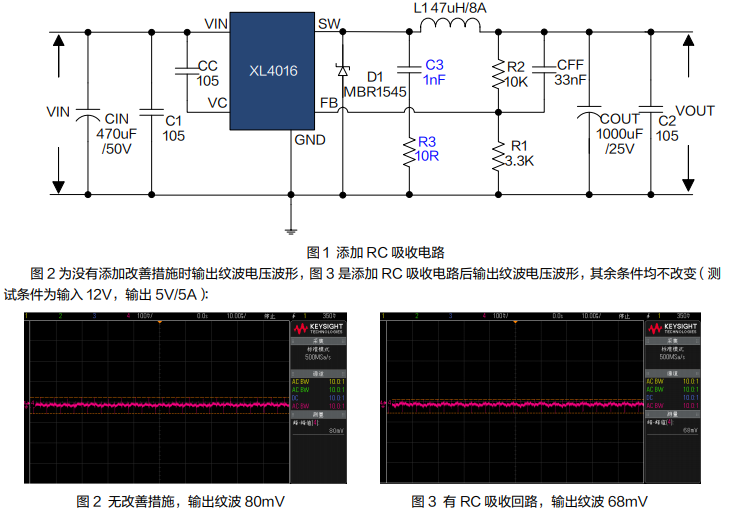
Figure 1 – Schematic with RC snubber circuit
Method 2: Add LC Filter at the Output
To further reduce output ripple, add an LC filter circuit at the output stage.
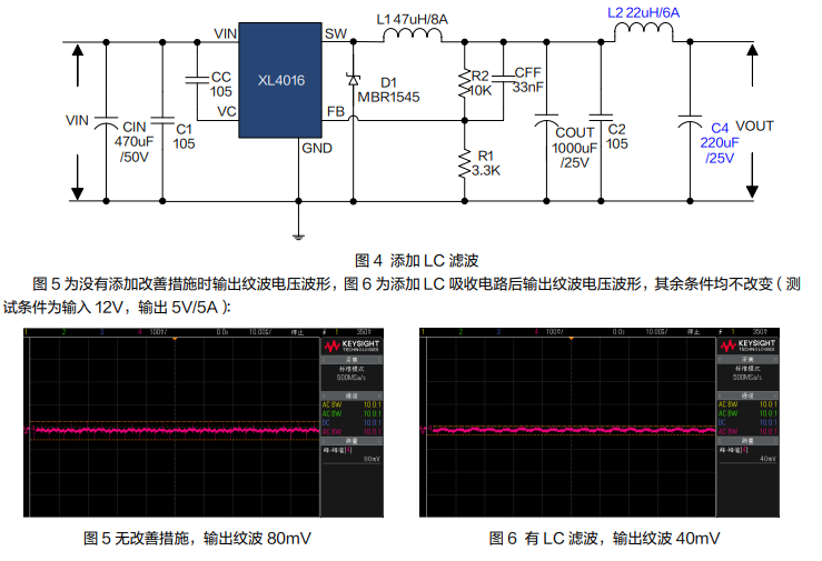
Figure 4 – Schematic with output LC filter
Method 3: Optimize PCB Routing to Reduce Parasitics
Parasitic parameters in switching power supplies are the root cause of most interference.
Key PCB rules:
- Minimize the switching current loop area.
- Use electrolytic + ceramic capacitors at the input; place ceramic caps close to VIN and GND.
- Route feedback traces away from switching nodes.
- Surround switching nodes with GND copper.
- Keep input capacitor positive near VIN; Schottky cathode near SW; Schottky anode near input capacitor negative.
About Maxipcb
Maxipcb empowers innovators to turn cutting-edge technologies into reality.
We offer one-stop solutions for design, simulation, testing, PCB manufacturing, component procurement and SMT assembly, enabling efficient development, rapid deployment and risk control across the full product lifecycle.Serving the world in communications, industrial automation, aerospace, automotive, semiconductor and beyond, we build a safer, more connected future together.


