In DCDC power supply circuit, PCB layout is very important for the realization of circuit functions and good indicators. Today, we take Buck circuit as an example to analyze how to make a reasonable PCB layout and the matters needing attention in design.
In DCDC power supply circuit, PCB layout is very important for the realization of circuit functions and good indicators. Today, we take Buck circuit as an example to analyze how to make a reasonable PCB layout and the matters needing attention in design.
1. power loopFigures 1(a) and 1(b) show the current loop when the upper tube is turned on and off, which is what we usually call the power loop. This part of the circuit is responsible for supplying power to the user's load and bears a large amount of power. The upper and lower transistors in the circuit generally use MOS transistors, which are controlled by PWM signals generated inside the chip for high-speed switching. The inductance and capacitance in the second half of the circuit constitute an LC filter circuit, so there will be no high current trend.

Figure 1(a) Figure 1(b)
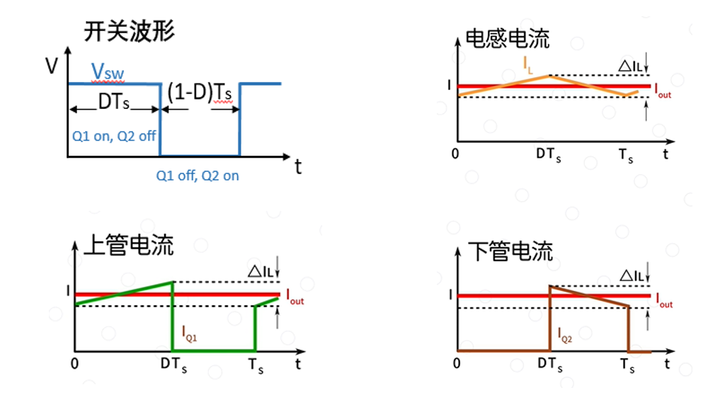
Figure 1(c)
Combining the current waveforms of the upper tube and the lower tube, that is, Q1 and Q2 (Figure 1(c)), it is not difficult to find that high current conversion rate will occur only in the parts of the two switching tubes. Due to the rapid change of voltage at PWM signal, strong noise will be generated at SW point. Therefore, we need to pay special attention to PCB wiring, and reduce the area of this rapidly changing link as much as possible to reduce the interference to other parts. Fortunately, with the progress of integration technology, most power chips have integrated the upper and lower tubes into the chip, and only a few applications need external MOS or diodes.
PCB layout of 02 power circuit
For a common buck chip, its inductive charging power loop includes input capacitor, upper tube MOSFET integrated inside the chip, power inductor and output capacitor. The inductive discharge power loop includes power inductor, output capacitor and lower tube MOSFET integrated in the chip.
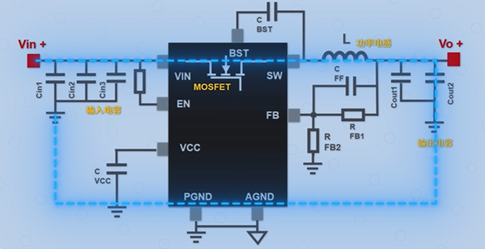
Figure 2(a) Inductor charging power circuit
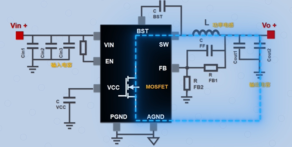
Figure 2(b) Inductor discharge power circuit
When wiring PCB, the wiring of these two power loops should be as short and thick as possible, and the loop area should be kept small under the condition of ensuring the current capacity, so as to reduce the noise radiated from the outside.
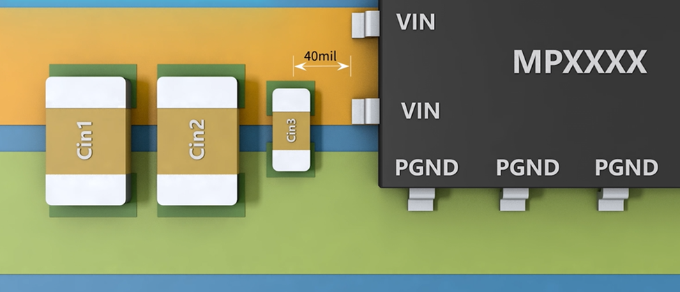
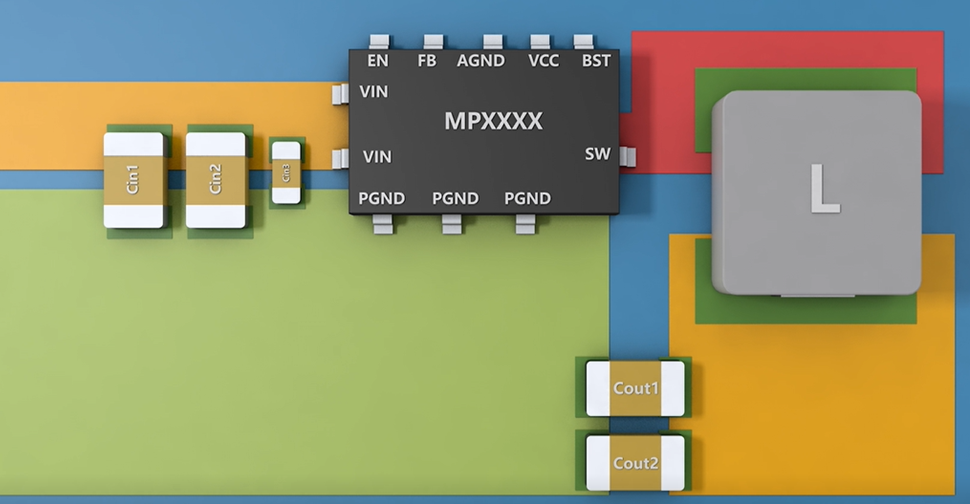
Input capacitance:It needs to be placed near the input Vin and power ground PGND of the chip to reduce the existence of parasitic inductance. Because the input current is discontinuous, the noise caused by parasitic inductance may exceed the withstand voltage of the chip and cause adverse effects on the logic unit. There should be at least one decoupling capacitor next to the VIN pin, and the distance is preferably less than 40mil, which is used to filter out the AC noise from the power input and the power noise from the chip (backward flow), and also plays the role of energy storage.
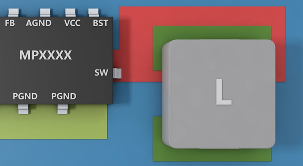
 SW point:
It is a switching node and a noise source, so we should keep the area as small as possible while ensuring the current and stay away from the easily disturbed signal wiring. In addition, it should be noted that for the Buck circuit with high current application, try not to punch holes at SW to avoid bringing noise to other layers.
 Output capacitance:
Similar to the input capacitor, the output capacitor needs to be placed near the output VOUT of the inductor and the power ground PGND, which is connected with the output capacitor in the shortest way and paved with copper to ensure the minimum power loop.
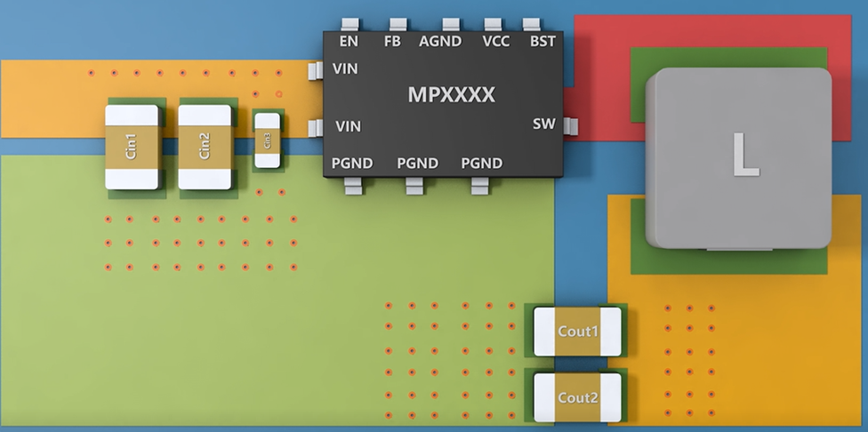
 Copper laying area and number of vias:
Both of them will affect the current flow and heat dissipation capacity of PCB. Generally, more holes need to be punched at VIN, Vout and GND, and the copper laying at these two places should be maximized to reduce the parasitic impedance, and the copper laying at SW should not be too small to avoid current limiting and lead to abnormal operation. Because the current-carrying capacity of PCB is related to PCB plate, thickness, wire width and thickness and temperature rise, it is complicated, so it can be accurately found and calculated through specific design specifications.
 3. PCB layout of logic circuit
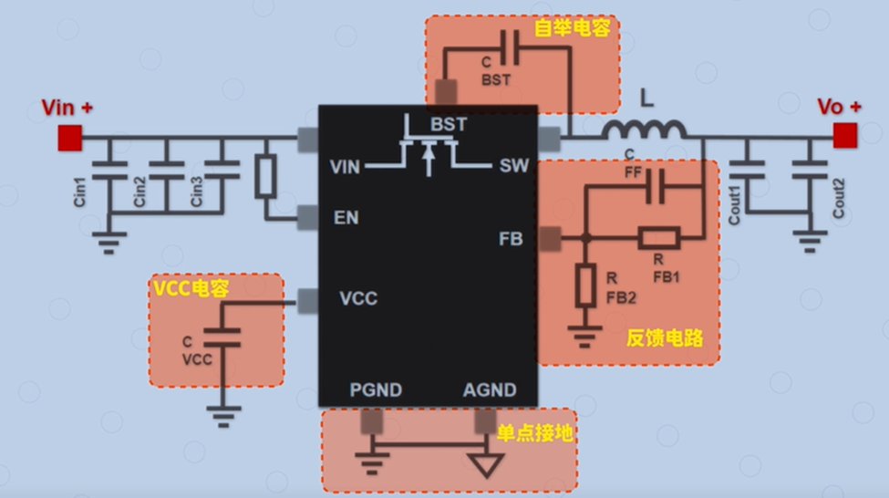
In buck circuit, we generally need to pay attention to the following logical links: bootstrap capacitor, feedback circuit, VCC and single point grounding.
 Bootstrap capacitance:
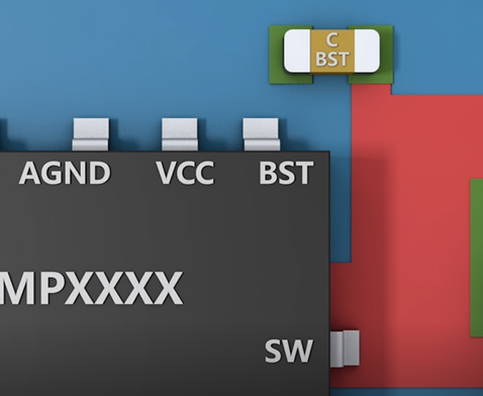
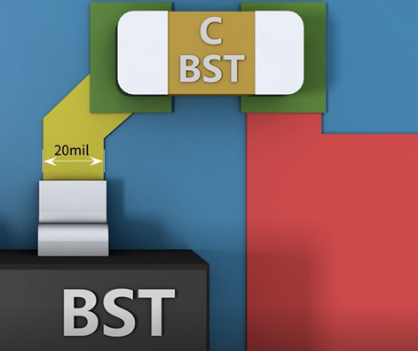
The upper tube integrated in the middle and high voltage buck chip is usually NMOS, so BST bootstrap circuit is needed. During the discharge of the inductor, by charging the bootstrap capacitor, a voltage higher than SW will be generated at the BST pin to drive the upper tube during the charging of the inductor. Therefore, BST, like SW, is also a point of high-speed voltage jump, which will radiate strong noise. Bootstrap capacitors should also be placed as close as possible to BST and SW to avoid the influence on other signals, and the width of wiring is generally 20mil.
 Feedback circuit:
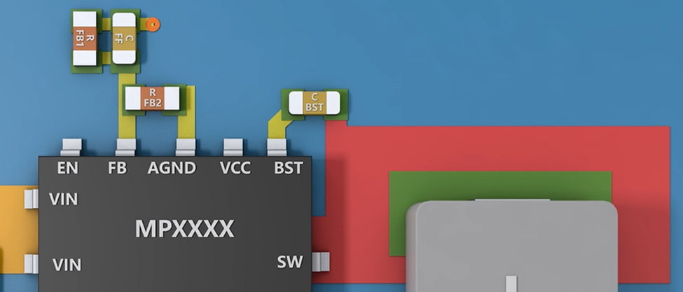
Generally, it includes FB upper and lower voltage dividing resistors and feedforward capacitors. Because the voltage at FB is very low, generally around 0.6-0.8V, it is easily confused with noise or ripple, which is the most sensitive and easily disturbed part of the chip and a common cause of system instability. Therefore, when wiring, the upper and lower voltage divider resistors and feedforward capacitors should be placed as close as possible to the chip to reduce noise coupling, and the wiring of FB resistor connected to FB pin should be as short as possible to reduce parasitic inductance and impedance. At the same time, it should be noted that the traces connecting FB to Vo can be set in other layers through vias, but they should be as far away from noise sources as possible, such as SW, BST, inductance, etc.
 VCC capacitance:
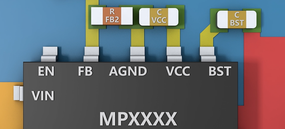
VCC supplies power to the logic circuit of the chip, which is the output of LDO inside the chip. The VCC capacitor should be placed between the VCC pin and GND pin of the chip nearby to stabilize the voltage. And the capacitor and the chip are on the same layer as far as possible, and no holes are punched.
 Single point grounding:
The ground of chips with large output current is generally divided into PGND and AGND, PGND is the power ground, and AGND is what we generally refer to as the signal ground, which is related to the logic parts of chips such as FB, EN and VCC. In order to prevent the power of the whole block from affecting the sensitive signal ground, it is suggested to connect AGND and PGND at a single point, or through a 0ohm resistor.
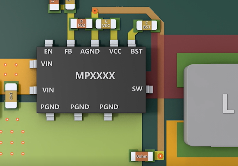
This is because although the bulk copper of PGND can absorb the noise of the input power supply, the noise radiated by PGND will still affect the sensitive logic circuit when the output current is large. The wiring mode of single point connection can provide a relatively "clean" ground for our logic circuit.
The above is what we need to pay attention to when drawing buck circuit PCB. When there is no way to draw a PCB, you can also open the specification of the chip first and check the PCB layout of the demo board or related guidance.
