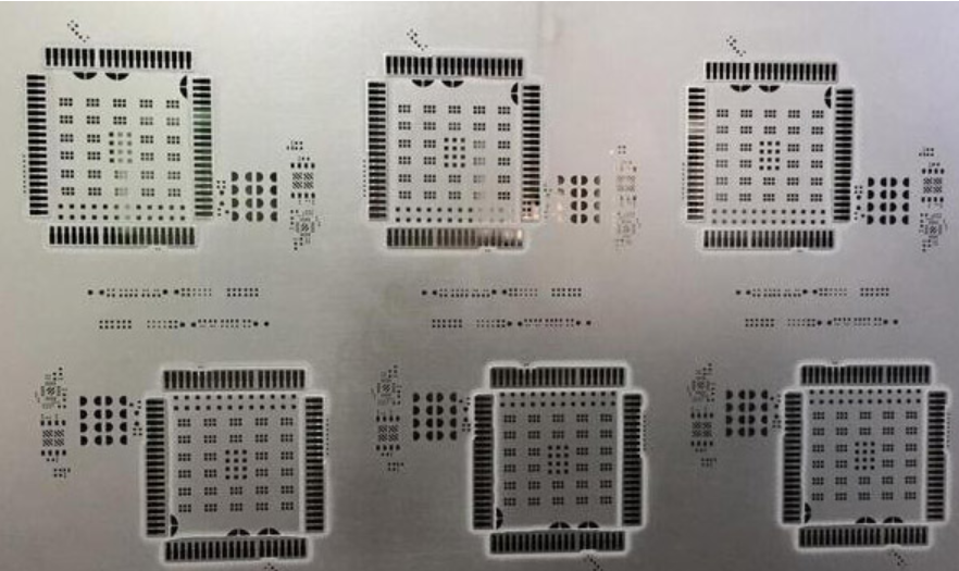
Those engaged in SMT assembly processing all know that stencils are used in the first process of PCBA assembly processing. The function of a stencil is to print solder paste onto the corresponding pads of the circuit board through the openings of the stencil by screen printing.
Those engaged in SMT assembly processing all know that stencils are used in the first process of PCBA assembly processing. The function of a stencil is to print solder paste onto the corresponding pads of the circuit board through the openings of the stencil by screen printing. First, the stencil is placed on the circuit board, then the stirred solder paste is placed on the stencil, and finally the solder paste is extruded by a scraper and drops onto the pads of the circuit board through the stencil openings. How do stencils affect the quality of SMT assembly processing?
1. Stencil Fabrication Methods
At present, the main stencil fabrication methods include: chemical etching, laser cutting, and electroforming.
Chemical etching has a large error and is not environmentally friendly; laser cutting features high data fabrication precision and little influence from objective factors, with trapezoidal openings facilitating demolding and enabling precision cutting, and it is moderately priced; electroforming results in smooth hole walls, making it particularly suitable for fabricating stencils for ultra-fine pitch components, but it is high-priced.
At present, most SMT processing factories adopt laser-cut stencils for their high cost performance and good quality.
2. Stencil Materials
Stencils are generally made of stainless steel, which offers high printing precision and a long service life.
3. Stencil Thickness
The thickness and size of a stencil directly determine the amount of solder paste on the pads, and thus directly affect the occurrence of soldering defects such as cold solder joints and solder bridges.
A single PCB usually has both components with a pitch of more than 1.27mm and fine-pitch components. Components with a pitch of more than 1.27mm require a 0.2mm-thick stainless steel stencil, while fine-pitch components need a 0.10-0.15mm-thick one. In such cases, the thickness of the stainless steel stencil can be determined according to the majority of components on the PCB, and then the amount of solder paste printed can be adjusted by expanding or reducing the opening size of the pads for individual components.
If the solder paste requirements of components on the same PCB vary greatly, the stencil can be locally thinned at the positions of fine-pitch components, but this thinning process incurs higher processing costs. Therefore, a compromise can be adopted by choosing a medium stencil thickness. For example, if some components on a PCB require a 0.20mm-thick stencil and others a 0.12-0.15mm-thick one, a 0.18mm-thick stainless steel stencil can be selected.
4. Stencil Opening Sizes
The opening size can be designed at a 1:1 ratio for general components. For large Chip components and PLCCs that require a large amount of solder paste, the opening area should be increased by 10%. For devices such as QFPs with a pin pitch of 0.5mm or 0.65mm, the opening area should be reduced by 10%.
5. Stencil Opening Shapes
Proper opening shapes can improve the mounting effect. For example, when the size of Chip components is smaller than 1005 or 0603, the distance between the two pads is very small, so the solder paste on the pads at both ends is likely to stick together at the bottom of the component during mounting, which easily leads to bridges and solder balls at the bottom of the component after reflow soldering.
Therefore, during stencil fabrication, the inner sides of a pair of rectangular pad openings can be modified into sharp-angled or arcuate shapes to reduce the amount of solder paste at the bottom of the component, thereby improving the solder paste adhesion at the component bottom during mounting.
6. Stencil Performance Requirements
- The frame must not be deformed.
- The tension should be uniform and high, preferably above 30N/mm².
- The metal sheet must be flat.
- The thickness error of the metal sheet should be within ±10%.
- The openings must be accurately aligned with the PCB (high precision).
- The cross-section of the stencil openings should be vertical, and the middle protruding part should not exceed 15% of the metal sheet thickness.
- The dimensional precision of the stencil openings for SMT assembly processing should be within a tolerance of ±0.01mm, and must not exceed 0.02mm.
The thickness and opening size of the stencil directly affect the printing amount of solder paste. During fabrication, parameters such as the stencil's thickness and opening size must be verified to ensure the quality of solder paste printing.
About Maxipcb
Maxipcb empowers innovators to turn cutting-edge technologies into reality.
We offer one-stop solutions for design, simulation, testing, PCB manufacturing, component procurement and SMT assembly, enabling efficient development, rapid deployment and risk control across the full product lifecycle.Serving the world in communications, industrial automation, aerospace, automotive, semiconductor and beyond, we build a safer, more connected future together.