This article focuses on PCB parasitic capacitance, including its effects, calculation methods and elimination measures.
This article focuses on PCB parasitic capacitance, including its effects, calculation methods and elimination measures.
1. What is PCB Parasitic Capacitance?
Parasitic capacitance has a general definition: it is an unintended virtual capacitance existing between two conductive structures separated by an insulator. It is a phenomenon in PCB layout where propagating signals behave as if a capacitor is present, even though no physical capacitor is actually designed there.
Parasitic capacitance typically occurs between any pair of conductors separated by a dielectric.
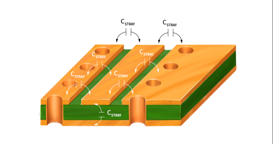
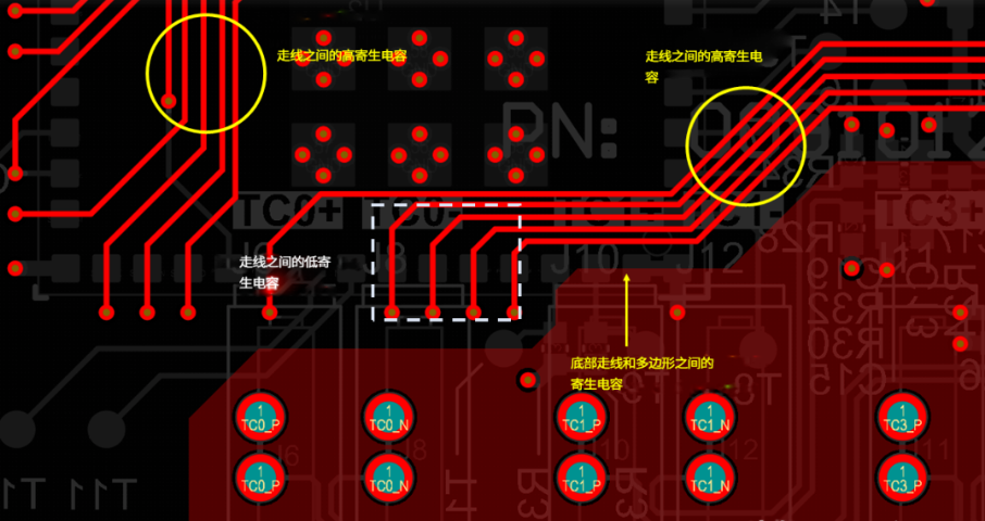 Note: Parasitic capacitance can exist on all layers of a PCB, not just the top layer as marked in the illustration, including areas with high/low parasitic capacitance between traces and parasitic capacitance between bottom traces and copper polygons.
2. The Effects of PCB Parasitic Capacitance
- Bandwidth limiting behavior in transmission lines, resulting in low-pass filter characteristics at very high frequencies
- Noise coupling between ground planes at different potentials, leading to common-mode noise
- Noise or signal coupling into components, especially wire-wound inductors
- High-frequency capacitive crosstalk (manifested as FEXT and NEXT)
- PDN impedance modification caused by the spacing between power and ground planes
- EMI coupling into heat sinks, generating common-mode currents
[Illustration position 2: Simple example of parasitic capacitance generation in PCB layout]
This illustration shows a conductor arrangement separated by an insulator in a PCB layout, forming a complex structure with equivalent capacitance. The structure can be modeled as an arrangement of capacitors, with additional parasitic inductance and resistance present. It is this equivalent capacitance and inductance that determine the impedance in the PCB layout.
3. How to Calculate PCB Parasitic Capacitance?
Parasitic capacitance is an inherent property of conductors, representing the charge storage per unit potential change. Its basic calculation formula is:
C = q/v
- C: Capacitance, Unit: Farad (F)
- V: Voltage, Unit: Volt (V)
- Q: Charge, Unit: Coulomb (C)
- For a constant electrical signal with no time variation (dv/dt = 0, i.e., no potential change):
i = 0
- If a capacitor exists in the circuit loop, dv/dt will converge to a fixed value, the potential changes, and a current is generated:
i ≠ 0
4. Calculation of Trace Capacitance
The capacitance of a parallel plate capacitor is given by:
C = (kA/11.3d) pFThe practical calculation formula for PCB trace capacitance is:
C = (0.00885ErA/d) pF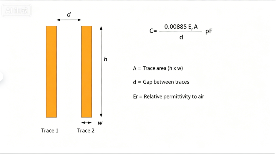 Parameters in the formula:
- A: Trace area (h×w, height × width of the trace)
- d: Gap between adjacent traces
- Er: Relative permittivity with respect to air
5. How to Reduce PCB Parasitic Capacitance?
Parasitic capacitance can never be completely eliminated in PCB layout, but it can be reduced, and measures can be taken to limit its impact on signal and power integrity.
Here are 10 practical measures to reduce parasitic capacitance in PCB layout:
01 Avoid parallel routing
Parallel routing maximizes the metal-to-metal area between traces, which in turn maximizes parasitic capacitance.
02 Remove unnecessary power planes
Power planes are generally considered AC ground (equivalent to ground planes), so removing redundant power planes is as important as removing ground planes near conductors.
03 Use Faraday shields or guard rings
Place Faraday shields between two traces to minimize the effects of parasitic capacitance.
04 Make critical traces as narrow and short as possible
To minimize parasitic capacitance, design critical traces to be as narrow as PCB manufacturing processes allow, and maintain a sufficient distance from adjacent traces.
05 Avoid excessive use of vias
Excessive vias increase parasitic capacitance; use surface-mount components instead of vias whenever possible.
06 Avoid improper component separation
Proper wiring between components, power/ground planes, and input/output ports is crucial for reducing unwanted parasitic capacitance.
07 Sandwich signal layers between two ground planes (or one ground/power plane)
For example, in a 4-layer PCB, place the power plane on the bottom layer and route sensitive traces between the power and ground planes. This prevents EMI from signals on one layer from inducing noise in signals on another layer.
08 Determine the appropriate layer thickness
Thinner layers reduce loop area and parasitic inductance, but increase parasitic capacitance—trade-offs are required based on design requirements.
09 Optimize signal integrity
Parasitic capacitance causes impedance reduction (usually due to close proximity to ground copper in layout), higher return loss (from impedance mismatch between interconnections and driver/receiver components), and higher insertion loss (from high-pass filtering behavior).
A simple solution is to increase the distance between interconnections and any conductors that are not the intended reference plane. During design, carefully calculate trace widths on the PCB, consider adjacent conductors (especially copper pours), and create coplanar trace arrangements. Calculate the minimum required gap between copper pours and traces to ensure impedance control.
10 Optimize power integrity
Parasitic capacitance has both positive and negative effects on power integrity, which can be analyzed by comparing PDN structures in PCBs with multiple grounding systems.
A common undesirable scenario for parasitic capacitance is in systems with multiple grounding points (e.g., PCB power ground plane, system ground area, and chassis ground). In such systems—especially high-current power supplies—parasitic capacitance may exist between the PCB ground plane and chassis ground, allowing common-mode current to flow through the system and generate strong radiation.
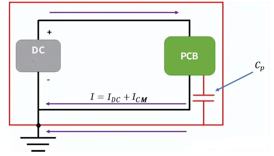
When there is a slight potential difference between the PCB ground plane and chassis ground, the parasitic capacitance of the equipment chassis forms a path for common-mode current.
6. Examples of Reducing PCB Parasitic Capacitance
01 High dV/dt Nodes in Switching Regulators
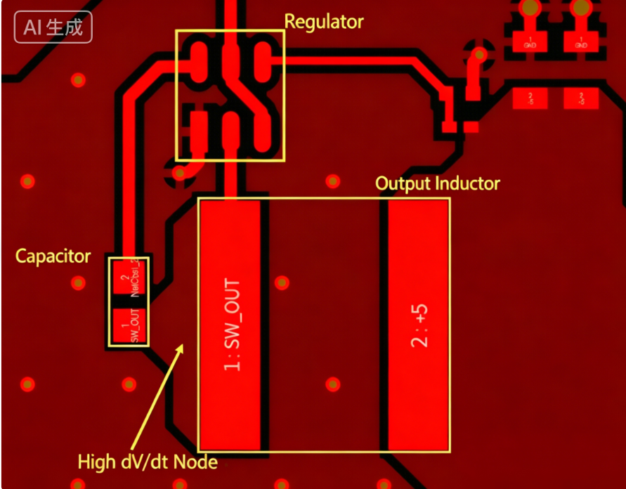
This regulator example illustrates the location of strong dV/dt nodes and why this layout leads to greater coupling to its feedback loop than to nearby parts of the system.
These nodes have parasitic capacitance to the adjacent ground area; if other components/circuits are nearby, this parasitic capacitance can introduce switching noise into those circuits. While a nearby ground plane provides some mitigation, the most effective way to prevent noise coupling is to connect a capacitor from the SW_OUT node back to the regulator chip. This large capacitor provides a low-impedance path for high dV/dt switching noise to return to the high side of the switching stage, effectively decoupling the switching stage output from GND.
Another effective strategy to reduce parasitic capacitance between SW_OUT and adjacent traces/circuits is to use a GND plane on the next layer. Placing the GND plane closer to the high dV/dt node reduces mutual capacitance by creating a stronger electric field coupling to GND, compared to coupling with other nodes in the PCB layout.
02 Mutual Capacitance Between Two Traces
Capacitive crosstalk is one of two types of coupling between traces (the other is inductive coupling), where a signal on one trace generates noise on another. At increasingly high frequencies, this is dominated by mutual capacitance. Two options to reduce this parasitic capacitance are:
- Place ground lines closer to the signal traces while narrowing the signal traces (maintaining a fixed impedance target)
- Increase the spacing between the signal traces


 Note: Parasitic capacitance can exist on all layers of a PCB, not just the top layer as marked in the illustration, including areas with high/low parasitic capacitance between traces and parasitic capacitance between bottom traces and copper polygons.

 Parameters in the formula:
 When there is a slight potential difference between the PCB ground plane and chassis ground, the parasitic capacitance of the equipment chassis forms a path for common-mode current.
 This regulator example illustrates the location of strong dV/dt nodes and why this layout leads to greater coupling to its feedback loop than to nearby parts of the system.
These nodes have parasitic capacitance to the adjacent ground area; if other components/circuits are nearby, this parasitic capacitance can introduce switching noise into those circuits. While a nearby ground plane provides some mitigation, the most effective way to prevent noise coupling is to connect a capacitor from the SW_OUT node back to the regulator chip. This large capacitor provides a low-impedance path for high dV/dt switching noise to return to the high side of the switching stage, effectively decoupling the switching stage output from GND.
This regulator example illustrates the location of strong dV/dt nodes and why this layout leads to greater coupling to its feedback loop than to nearby parts of the system.
These nodes have parasitic capacitance to the adjacent ground area; if other components/circuits are nearby, this parasitic capacitance can introduce switching noise into those circuits. While a nearby ground plane provides some mitigation, the most effective way to prevent noise coupling is to connect a capacitor from the SW_OUT node back to the regulator chip. This large capacitor provides a low-impedance path for high dV/dt switching noise to return to the high side of the switching stage, effectively decoupling the switching stage output from GND.