On computer memory modules and graphics cards, we can see a row of golden conductive contacts – these are called "Gold Fingers".
In PCB design and manufacturing, Gold Fingers (also known as Edge Connectors) serve as the interface for board‑to‑external‑network connections via connector mating.
On computer memory modules and graphics cards, we can see a row of golden conductive contacts – these are called "Gold Fingers".
In PCB design and manufacturing, Gold Fingers (also known as Edge Connectors) serve as the interface for board‑to‑external‑network connections via connector mating.
Let us now explore the treatment methods and some detail considerations for Gold Fingers in PCBs.
Surface Finishes for Gold Finger PCBs
1. Electroplated Nickel Gold:
Thickness can reach 3‑50 µ". Due to its excellent conductivity, oxidation resistance, and wear resistance, it is widely used on Gold Finger PCBs that require frequent insertion/removal or are subject to regular mechanical friction. However, because electroplated gold is very expensive, it is typically applied only locally to areas such as Gold Fingers.
2. ENIG (Electroless Nickel Immersion Gold):
Standard thickness is 1 µ", with a maximum of 3 µ". Owing to its good conductivity, flatness, and solderability, ENIG is widely used on high‑precision PCBs with features such as keypads, wire‑bonded ICs, and BGAs. For Gold Finger PCBs that do not have high wear‑resistance requirements, ENIG over the entire board is also an option. ENIG is significantly less costly than electroplated gold. The colour of the ENIG finish is golden yellow.
Detail Considerations for Gold Fingers in PCBs
-
To enhance wear resistance, Gold Fingers typically require electroplated hard gold.
-
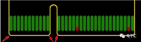
Gold Fingers require chamfering, usually at 45°. Other angles such as 20° or 30° are also used. If the design does not include a chamfer, it is a problem. A 45° chamfer on a PCB is shown in the figure below:
-
The entire Gold Finger area should have the solder mask opened (no solder mask coverage). No stencil opening (solder paste) is required for the pins.
-
ENIG or Immersion Silver pads should be at least 14 mil away from the tip of the Gold Finger. It is recommended to maintain a minimum distance of 1 mm between pads (including via pads) and the Gold Finger edge.
-
Do not pour copper on the surface layer (top layer) of the Gold Finger area.
-
On all inner layers of the Gold Finger area, the copper should be recessed (copper pull‑back). Typically, the pull‑back width should be at least 3 mm. Both half‑finger and full‑finger copper pull‑back are acceptable.
Is the "Gold" in Gold Fingers Real Gold?
First, let us clarify two concepts: soft gold and hard gold.
-
Soft gold generally refers to pure gold, which is relatively soft.
-
Hard gold refers to gold compounds that are harder in nature.
The primary function of Gold Fingers is to provide electrical connection, so they must have good conductivity, wear resistance, oxidation resistance, and corrosion resistance. Because pure gold is relatively soft, Gold Fingers are not made of pure gold; instead, they are plated with a layer of "hard gold" (a gold compound). This provides the excellent conductivity of gold while also delivering the required wear and oxidation resistance.
So, is "soft gold" ever used on PCBs? The answer is yes – for example, on contact surfaces of mobile phone keypads, and for aluminium wire bonding on COB (Chip‑on‑Board) assemblies. Soft gold is typically deposited by electroplating a nickel‑gold layer on the board, and its thickness can be controlled with good flexibility.
Tip: Whether it is soft gold or hard gold plated on a PCB, the quantity is very small. So please do not dismantle electronic devices to "collect gold"!
About Maxipcb
Maxipcb empowers innovators to turn cutting-edge technologies into reality.We offer one-stop solutions for design, simulation, testing, PCB manufacturing, component procurement and SMT assembly, enabling efficient development, rapid deployment and risk control across the full product lifecycle.
Serving the world in communications, industrial automation, aerospace, automotive, semiconductor and beyond, we build a safer, more connected future together.
