
The power supply is often the most easily overlooked part of circuit design. In a well‑designed product, the power supply should be a critical element, as it greatly affects the overall system performance and cost. The use of capacitors in power supply design is, in turn, the most frequently neglected aspect of the power supply itself.
I. Operating Principle of Capacitors in Power Supply Design
In power supply applications, capacitors are mainly used for filtering and decoupling/bypassing. Filtering is the operation of removing a specific band of frequencies from a signal and is an important measure for suppressing and preventing interference. It originates from communication theory, where it is a technique for extracting a desired signal from a received signal that contains noise – the “received signal” corresponds to the observed random process, and the “desired signal” to the estimated random process.
Filtering primarily refers to eliminating external noise, whereas decoupling/bypassing (hereafter referred to simply as “decoupling”) reduces the noise that a local circuit radiates to the outside. Many people easily confuse the two. Let us look at the following circuit structure:
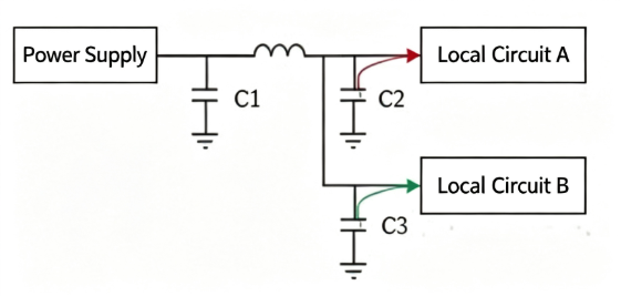
In this circuit, the power supply provides power to both A and B. The current flows through C1, then passes through a PCB trace and splits into two paths to supply A and B respectively. When A suddenly needs a large current at a certain instant, without C2 and C3, the voltage at node A would drop due to the line inductance, and the voltage at node B would also decrease because it is affected by the voltage at A. Thus, the current change in local circuit A causes a variation in the supply voltage of local circuit B, interfering with the signal in B. Likewise, current changes in B will interfere with A. This is called “common‑path coupling interference.”
After adding C2, when local circuit A needs a transient large current, capacitor C2 can temporarily supply current to A. Even though the common‑path inductance still exists, the voltage at node A does not drop too much, and the impact on B is greatly reduced. In this way, bypass current achieves decoupling.
Generally, filtering uses large‑value capacitors, which do not require very fast response but need relatively large capacitance. If local circuit A in the figure refers to a chip, the capacitor should be placed as close as possible to the chip’s power pin. If “local circuit A” refers to a functional module, ceramic capacitors can be used; if the capacitance is insufficient, tantalum capacitors or aluminium electrolytic capacitors may be used (provided that each chip in the functional module already has its own decoupling capacitor – a ceramic capacitor).
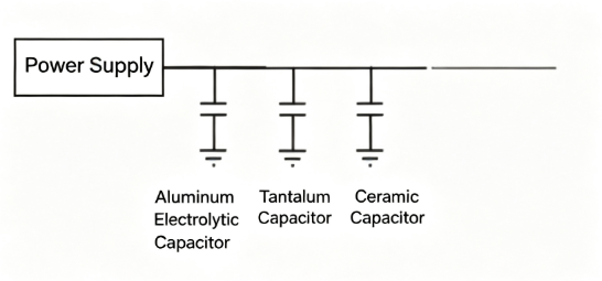
The capacitance value for filtering can often be found from the calculation formula in the power supply IC data sheet. If the filtering circuit uses electrolytic, tantalum, and ceramic capacitors together, place the electrolytic capacitor closest to the switching power supply to protect the tantalum capacitor, and place the ceramic capacitor behind the tantalum capacitor. This yields the best filtering effect.
A decoupling capacitor must meet two requirements: capacitance value and ESR (equivalent series resistance). This means that a single 0.1 µF capacitor may not decouple as well as two 0.01 µF capacitors. Moreover, a 0.01 µF capacitor has lower impedance at higher frequencies; within those frequency ranges, if a 0.01 µF capacitor meets the capacitance requirement, it will provide better decoupling than a 0.1 µF capacitor.
Many high‑speed chips with numerous pins provide design guidelines for decoupling capacitors in their power supply recommendations. For example, a 500‑pin BGA package may require at least 30 ceramic capacitors for the 3.3 V supply, plus several large capacitors, with a total capacitance above 200 µF…
II. Proper Selection of Capacitors for Various Power Supplies
As basic components, capacitors play an important role in electronic circuits. In traditional applications, they are mainly used for bypass coupling, power filtering, DC blocking, and oscillation/delay in small‑signal circuits. With the development of electronic circuits, especially power electronics, different application scenarios impose specific requirements on capacitors.
Starting from the capacitor structure: the simplest capacitor consists of two terminal plates and an insulating dielectric (including air) between them. When energised, the plates become charged, creating a voltage (potential difference); however, because of the insulating material, the entire capacitor is non‑conductive. This holds true provided that the voltage does not exceed the capacitor’s critical voltage (breakdown voltage). As we know, any material is relatively insulating; when the voltage across it increases to a certain level, it can become conductive. That voltage is called the breakdown voltage.
Capacitors are no exception – after breakdown, they are no longer insulators. However, in basic education contexts, such voltages are not encountered in circuits, so capacitors operate below the breakdown voltage and can be treated as insulators. But in AC circuits, because the current direction varies as a function of time, the capacitor charging and discharging process takes time, and a changing electric field forms between the plates, which is also a function of time.
1. Filtering Capacitors
After rectification of AC (mains or high‑frequency), capacitors are needed for filtering to smooth the output voltage, requiring large capacitance. Aluminium electrolytic capacitors are generally used. The main concern with aluminium electrolytic capacitors is the relationship between temperature and lifetime, which basically follows the “10‑degree rule” (i.e., lifetime doubles for every 10°C reduction). Therefore, in many high‑temperature and high‑reliability applications, long‑life electrolytic capacitors (e.g., 5000 h or more, even 105°C, 5000 h) should be selected. Generally, smaller‑size electrolytic capacitors have shorter lifetimes.
For input filtering capacitors in DC/DC switching regulators, because the switching converter draws energy from the supply in pulses, relatively large high‑frequency currents flow through the filter capacitor. If the electrolytic capacitor has a large ESR, it will generate significant losses, causing heating. Low‑ESR electrolytic capacitors can significantly reduce heating caused by ripple current (especially high‑frequency ripple).
For electrolytic capacitors used in output rectification of switching regulators, their impedance‑frequency characteristics should not show an upward trend even at 300 kHz or 500 kHz. Ordinary electrolytic capacitors already start to rise after 100 kHz, so their performance in output filtering for switching supplies is relatively poor. In experiments, it was found that a common CDII type 4700 µF, 16 V electrolytic capacitor did not produce lower ripple and spikes than a CD03HF type 4700 µF, 16 V high‑frequency electrolytic capacitor when used for switching supply output filtering; moreover, the ordinary electrolytic capacitor had a higher temperature rise. For sudden load changes, the transient response of the ordinary electrolytic capacitor was far inferior to that of the high‑frequency type.
Since aluminium electrolytic capacitors do not perform well at high frequencies, they should be complemented by ceramic or non‑inductive film capacitors, which have excellent high‑frequency characteristics and low ESR. For example, an MMK5 type 1 µF capacitor has a resonant frequency above 2 MHz and an equivalent impedance below 0.02 Ω, much lower than that of an electrolytic capacitor. Moreover, the smaller the capacitance, the higher the resonant frequency (up to 50 MHz or more), thus achieving good output frequency response or dynamic response for the power supply.
Among filtering capacitors, we focus here on how to select filter capacitors in switching power supplies.
How to select filter capacitors in switching power supplies
Filter capacitors play a vital role in switching power supplies. How to correctly choose filter capacitors, especially output filter capacitors, is a major concern for engineers.
Ordinary electrolytic capacitors used in 50 Hz mains circuits have a ripple voltage frequency of only 100 Hz, and charge/discharge times are in milliseconds. To obtain a smaller ripple coefficient, the required capacitance can reach hundreds of thousands of microfarads. Therefore, ordinary low‑frequency aluminium electrolytic capacitors are designed primarily to increase capacitance; capacitance, dissipation factor, and leakage current are the main parameters for evaluating their quality. In contrast, the output filter electrolytic capacitor in a switching power supply has a sawtooth voltage frequency of tens of kilohertz or even tens of megahertz. At such frequencies, capacitance is not the primary indicator; the key metric is the impedance‑frequency characteristic. It requires a low equivalent impedance within the switching power supply’s operating frequency range, and it must also effectively filter the high‑frequency spikes generated by semiconductor devices during operation.
Many electronic designers know the role of filter capacitors in power supplies, but the filter capacitors used at the output of a switching supply differ from those used in mains‑frequency circuits. In a mains‑frequency circuit, the ripple voltage is only 100 Hz, with millisecond charge/discharge times, and to achieve a low ripple coefficient, the capacitance must be very large (hundreds of thousands of µF). Thus, ordinary low‑frequency aluminium electrolytic capacitors are manufactured with an emphasis on capacitance, and the main quality indicators are capacitance, dissipation factor, and leakage current.
For an electrolytic capacitor used as an output filter in a switching regulator, the sawtooth voltage frequency can be tens of kilohertz or even tens of megahertz. Its requirements are different from low‑frequency applications: capacitance is not the primary factor; rather, its impedance‑frequency characteristic determines its performance. It must have low impedance across the switching regulator’s operating frequency band, and it must also effectively filter the high‑frequency spike noise (up to hundreds of kilohertz) generated by semiconductor devices. Ordinary low‑frequency electrolytic capacitors begin to exhibit inductive impedance around 10 kHz and cannot meet the demands of switching power supplies.
Ordinary low‑frequency electrolytic capacitors become inductive around 10 kHz and cannot satisfy switching supply requirements. Specialised high‑frequency aluminium electrolytic capacitors for switching supplies have four terminals: both ends of the positive aluminium foil are brought out as the positive terminals, and both ends of the negative foil as the negative terminals. Current enters from one positive terminal, passes through the capacitor, and exits from the other positive terminal to the load; the return current from the load enters from one negative terminal and exits from the other to the supply negative.
Specialised high‑frequency aluminium electrolytic capacitors for switching regulators have four terminals. The current from the regulator enters from one positive terminal, goes through the capacitor, and flows from the other positive terminal to the load; the return current from the load enters from one negative terminal and flows out from the other to the supply negative. Because these four‑terminal capacitors have excellent high‑frequency characteristics, they provide a very effective means of reducing output voltage ripple and suppressing switching spike noise.
Switching regulators often include multi‑function comprehensive protection: besides the basic voltage stabilisation function, they should also have overvoltage protection (above +10% of output voltage), undervoltage protection (below ‑10%), phase‑loss protection, and short‑circuit/overload protection. Spike suppression (optional): sometimes the grid produces high‑amplitude, narrow pulses that can puncture low‑voltage‑withstand electronic components. The surge suppression module in a regulated power supply can effectively suppress such spikes.
High‑frequency aluminium electrolytic capacitors also come in multi‑section forms, where the aluminium foil is divided into shorter segments with multiple parallel connection tabs to reduce the resistive component of the capacitive reactance. In addition, low‑resistivity materials and screw terminals are used to enhance the capacitor’s ability to withstand large currents.
Stacked‑film capacitors, also called non‑inductive capacitors, have a structure similar to a book, unlike ordinary electrolytic capacitors whose windings are cylindrical and have relatively large equivalent series inductance. In stacked capacitors, the magnetic fluxes generated by the currents cancel each other, reducing the inductance and providing superior high‑frequency characteristics. Such capacitors are often square for easy mounting and can also save space.
2. Snubber and Commutation Capacitors
As gate‑controlled semiconductor devices increase in power rating, switching speed, and voltage rating, the capacitors used in snubber circuits must do more than just provide sufficient voltage rating, capacitance, and excellent high‑frequency characteristics.
In high‑power power electronics, with IGBT switching speeds below 1 µs, it is quite common for snubber capacitors to withstand voltage change rates dv/dt of several V/µs or even tens of V/µs. Ordinary capacitors, especially ordinary metallised capacitors, have dv/dt < 100 V/µs; special metallised capacitors have dv/dt ≤ 200 V/µs; dedicated dual‑metallised capacitors of small capacitance (<10 nF) have dv/dt ≤ 1500 V/µs, and larger capacitance (<0.1 µF) have about 600 V/µs. Under such huge and repetitive peak current surges, they are difficult to withstand and can damage power electronics.
Currently, snubber‑specific capacitors with metal‑foil electrodes can withstand large peak and RMS currents. For example, smaller‑capacitance types (below 10 nF) can withstand voltage change rates of 100,000 V/µs to 455,000 V/µs, peak currents of 3700 A, and RMS currents up to 9 A (e.g., CDV30FH822J03); larger‑capacitance (above 10 nF, below 0.47 µF) or larger‑size types can withstand dv/dt above 3400 V/µs and peak currents of 1000 A.
Thus, although both are non‑inductive capacitors, metallised and metal‑foil capacitors behave quite differently in snubber applications; they may look similar but are by no means interchangeable. Capacitor size affects its dv/dt and peak current capability – generally, longer length yields lower dv/dt and peak current ratings.
Snubber circuits operate with high peak currents but low duty cycles, so the RMS current is not extremely high. Similar conditions apply to commutation capacitors in thyristor inverters, though these require lower dv/dt but higher peak and RMS currents, and ordinary capacitors cannot meet the current requirements.
In some special applications, energy‑storage capacitors must discharge repeatedly and rapidly into very low‑resistance, low‑inductance loops. In such cases, only parallel combinations of snubber capacitors can ensure long‑term reliability.
3. Resonant Capacitors
In resonant converters, such as resonant switching power supplies or the resonant tanks of thyristor medium‑frequency power supplies, the resonant capacitors often carry large currents. Similarly, in electronic ballasts, if the resonant capacitor is improperly chosen, even if the voltage does not reach breakdown, the capacitor may be damaged due to excessive resonant current.
In circuits containing both capacitors and inductors, when they are connected in parallel, there may be brief intervals where the capacitor voltage gradually rises while its current decreases, and simultaneously the inductor current gradually increases while its voltage decreases. In another short interval, the opposite occurs. The voltage can reach a positive maximum and a negative maximum, and the current direction also changes. This phenomenon is called electrical oscillation.
Oscillations may decay or persist. When they persist with constant amplitude, it is called sustained oscillation, or resonance. The time for one complete cycle of voltage change across the capacitor or inductor during resonance is the resonant period, and its reciprocal is the resonant frequency – hence the definition.
In summary, in modern power supply technology, different applications require capacitors with different characteristics. They cannot be mixed, misused, or wrongly selected. Only proper selection can prevent unnecessary failures and ensure product performance.
III. Design Example of a Capacitive Dropper Power Supply
The conventional method to convert AC mains to low‑voltage DC is to use a transformer for step‑down followed by rectification and filtering. When size and cost constraints limit the use of a transformer, the simplest and most practical approach is the capacitive dropper power supply.
1. Circuit Principle of the Capacitive Dropper Supply
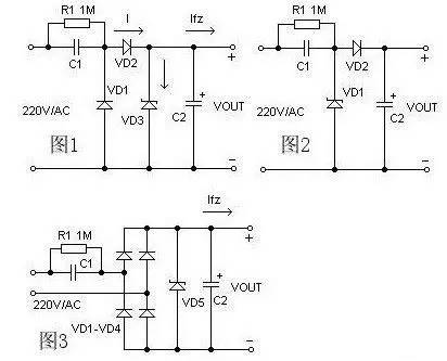
The basic circuit of a capacitive dropper supply is shown in Figure 1. C1 is the dropping capacitor, D2 is the half‑wave rectifier diode, D1 provides a discharge path for C1 during the negative half‑cycle of the mains, D3 is the Zener diode, and R1 is the discharge resistor for C1 after power‑off. In practice, the circuit shown in Figure 2 is more commonly used. When a larger load current is required, the bridge rectifier configuration of Figure 3 can be used. The unregulated DC voltage after rectification is generally above 30 V and fluctuates greatly with load current changes, because such supplies have high internal impedance. Therefore, they are not suitable for high‑current applications.
2. Component Selection Guidelines for Capacitive Dropper Circuits
(1) When designing the circuit, first determine the exact load current, then choose the dropping capacitor value with reference to design examples. Excess current beyond the load requirement flows through the Zener diode; if the diode’s maximum allowable current Idmax is less than Ic – Io, the Zener diode may be damaged.
(2) To ensure reliable operation of C1, its voltage rating should be greater than twice the mains voltage.
(3) The discharge resistor R1 must be chosen so that the charge on C1 is discharged within the required time.
3. Design Example
In Figure 2, given C1 = 0.33 µF, AC input = 220 V / 50 Hz, find the maximum load current the circuit can supply.
The capacitive reactance Xc of C1 is:
Xc = 1 / (2 π f C) = 1 / (2 × 3.14 × 50 × 0.33 × 10⁻⁶) = 9.65 kΩ
The charging current (Ic) through C1 is:
Ic = U / Xc = 220 / 9.65 = 22 mA
As a rule of thumb, the relationship between the dropping capacitor C1 (in µF) and the load current Io (in A) can be approximated as:
C = 14.5 × Io
where C is in µF and Io is in A.
About Maxipcb
Serving the world in communications, industrial automation, aerospace, automotive, semiconductor and beyond, we build a safer, more connected future together.