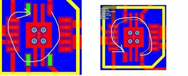
In engineering, mistakes are inevitable. Learning from mistakes is the fastest way to grow—and PCB design is no exception. This article summarizes the most common mistakes in PCB design.
In engineering, mistakes are inevitable. Learning from mistakes is the fastest way to grow—and PCB design is no exception. This article summarizes the most common mistakes in PCB design.
1. Pin Definition Errors
Linear voltage regulators are cheaper than switching power supplies but have lower power conversion efficiency. Due to their ease of use and cost-effectiveness, many engineers choose linear regulators for their designs.
However, it’s important to note that while convenient, linear regulators consume significant power and generate substantial heat. In contrast, switching power supplies are more complex to design but offer higher efficiency.
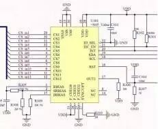
A critical mistake to avoid: the output pins of some voltage regulators may be incompatible with each other. Always verify the pin definitions in the chip datasheet before routing.
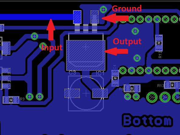 Figure 1.1: A linear voltage regulator with a special pin arrangement
2. Routing Errors
Discrepancies between the design intent and actual routing are major sources of errors in the final stages of PCB design. Thorough cross-checks are essential, including:
- Component dimensions
- Via quality
- Pad sizes
- Review levels
In short, repeatedly verify all details against the schematic to ensure consistency.
3. Acid Traps
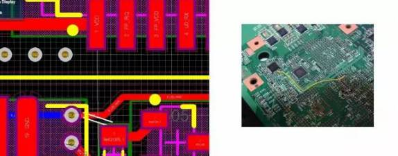
When the angle between PCB traces is too small (forming an acute angle), an "acid trap" may occur.
During the PCB etching process, etchant can become trapped in these sharp corners, removing more copper than intended. This can create weak points or "traps" that may lead to trace breakage and open circuits later. Modern manufacturing processes using photosensitive etching solutions have significantly reduced the occurrence of acid traps, but the risk remains if proper routing practices are ignored.
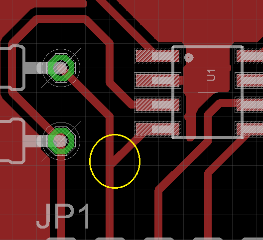 Figure 3.1: Traces with acute connection angles (prone to acid traps)
4. Tombstoning Components
During reflow soldering of small surface-mount devices (SMDs), components may lift at one end due to uneven solder wetting—a phenomenon commonly known as "tombstoning."
This issue is typically caused by asymmetric routing patterns, which result in uneven heat distribution across the component’s pads. Implementing proper DFM (Design for Manufacturing) checks can effectively mitigate tombstoning.
5. Trace Width Mismatch
When the current through a PCB trace exceeds 500mA, standard trace widths may become insufficient. Generally, traces on the PCB surface can carry more current than inner-layer traces of the same thickness and width—this is because surface traces dissipate heat through air circulation.
Trace width requirements also depend on the copper foil thickness of the layer. Most PCB manufacturers offer copper foil thickness options ranging from 0.5 oz/sq.ft to 2.5 oz/sq.ft, and trace widths must be adjusted accordingly to handle the expected current.
6. Additional Common Mistakes
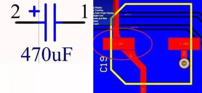
- Reversed pins for polarized capacitors: Mixing up the positive and negative pins of polarized capacitors in the schematic or PCB layout.
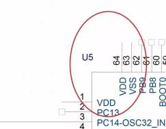
- Missing or reversed power/ground connections: Forgetting to connect power (VDD) and ground (VSS) pins, or reversing their connections.
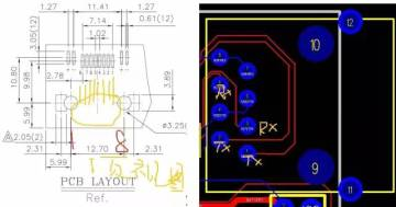
- Incorrect connector pinout: Mixing up the wire order of connectors (e.g., serial ports, power connectors).
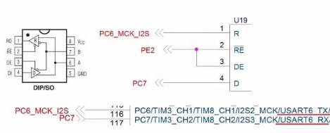
- Reversed RX/TX signals: Swapping the receive (RX) and transmit (TX) pins in UART, SPI, or other communication interfaces.
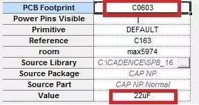
- Non-existent component footprints: Creating custom footprints without verifying if the corresponding components are commercially available (e.g., downloading datasheets from untrusted sources only to find the component cannot be purchased).
- Copying circuits with unavailable components: Blindly copying reference circuits (e.g., from brand-name products) without confirming component availability. For example, a smart lock team once copied a Samsung smart lock circuit but struggled to source a Korean-made capacitive touch controller with no domestic distributors or technical support.
- Ignoring capacitor voltage rating: Selecting capacitors based solely on capacitance without considering voltage rating, leading to situations where a capacitor meeting the voltage requirement cannot fit in the allocated footprint.
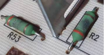
- Ignoring resistor power rating: Choosing resistors based only on resistance value without accounting for power dissipation, which can result in resistor overheating and failure.
- Neglecting DRC reports: Relying solely on visual inspection of ratnest lines instead of reviewing Design Rule Check (DRC) reports, leading to manufacturing defects.
- Reversed component footprints: Designing or placing component footprints in reverse (e.g., flipping a dual-in-line package horizontally).
- Unprocessed thermal pad solder mask: Failing to remove the solder mask from thermal pads, preventing effective heat dissipation and proper soldering.
 About Maxipcb
Maxipcb empowers innovators to turn cutting-edge technologies into reality.
We offer one-stop solutions for design, simulation, testing, PCB manufacturing, component procurement and SMT assembly, enabling efficient development, rapid deployment and risk control across the full product lifecycle.Serving the world in communications, industrial automation, aerospace, automotive, semiconductor and beyond, we build a safer, more connected future together.