This article analyzes the impact of the connection (or non-connection) between a PCB working ground and a metal enclosure on ESD interference through a practical case study.
This article analyzes the impact of the connection (or non-connection) between a PCB working ground and a metal enclosure on ESD interference through a practical case study.
Part 1 Phenomenon Description
An electronic device features the basic product architecture as shown below.
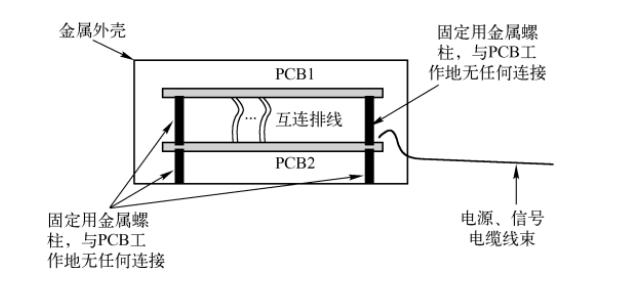
As can be seen from the diagram:
- The product is housed in a metal enclosure.
- Two PCBs are installed inside the device and fixed to the metal enclosure via metal studs.
- No electrical connection exists between the studs and the circuits or working ground on the PCBs.
- Signal interaction between the two PCBs is realized through a flat cable.
- An I/O connector is mounted on PCB2, and the interconnected cable harness carries power signals, input/output signals and other control signals.
When the product underwent contact discharge testing in accordance with the test configuration specified in the ISO 10605 standard, it was found that system errors occurred whenever the test voltage exceeded ±2 kV.
There is no need to panic when facing ESD issues—essentially, such problems can be resolved through proper grounding of the equipment.
Why did the device fail the test in this case? A detailed analysis is provided below.
Part 2 Cause Analysis
Based on the aforementioned product architecture, we can map out the ESD common-mode interference path when electrostatic discharge occurs on the metal enclosure, as shown in the diagram below:
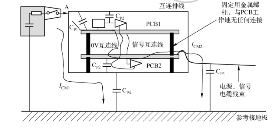
Two ESD common-mode interference paths are shown in the diagram, namely the path of ICM1 on the left and the path of ICM2 on the right.
It is evident that the second interference path (ICM2) is the primary cause of the ESD test failure.
The ICM2 interference path passes through PCB1, the flat cable between PCB1 and PCB2, PCB2, and the interconnected cable harness on PCB2.
This constitutes an undesired interference path—the larger the interference current in this path, the greater the interference on the PCBs and the higher the probability of malfunctions.
For ease of understanding, the interference path can be simplified as shown below:
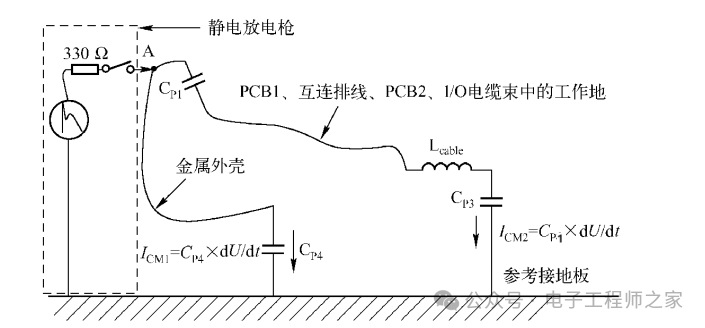
Key Parasitic Capacitance Definitions
- CP1: Parasitic capacitance between the product's metal enclosure and the PCB1 ground plane.
Note: Parasitic capacitance is generated between the metal enclosure and the components, printed traces, ground plane and power plane on PCB1. Among these, the parasitic capacitance between the metal enclosure and the ground/power plane is the largest (e.g., 10 pF).
- CP3: Parasitic capacitance between the product's cable harness and the reference ground plate.
In the test, the cable harness is typically placed 25 mm above the reference ground plate, and this capacitance can be estimated at 60 pF/m (per the cable placement requirements in the ISO 10605 standard). The cable harness in this case is 2 meters long, so CP3 is estimated to be 120 pF.
- CP4: Parasitic capacitance between the product's metal enclosure and the reference ground plate.
During the test, the product was placed on the reference ground plate and isolated by an insulator with a relative permittivity of less than 1.4 and a height of 25 mm; this capacitance is approximately 30 pF.
- CP2: Parasitic capacitance between the PCB2 ground plane and the metal enclosure.
In the circuit, CP2 is connected in series with CP4, and this series combination is in parallel with CP3, with CP2 << CP4.
It can thus be concluded that the voltage at the ESD discharge point Point A relative to the reference ground plate is not zero (when the metal enclosure is properly connected to the reference ground plate, the voltage at Point A relative to the reference ground plate is close to zero).
During the 4 kV contact discharge test, the transient voltage at Point A can reach 1 kV, which generates a common-mode current
ICM2. The formula for calculating the common-mode current is as follows:
ICM2=CP1×dU/dt=10 pF×1 kV/1 ns=10 A
Note: At the frequency of the ESD interference current, the equivalent characteristic impedance caused by the cable (Lcable) and CP4 is approximately 150 Ω, which is much lower than the capacitive reactance of CP1.
Interpretation of ESD Common-Mode Interference Current ICM2
When electrostatic discharge occurs, equipotentiality cannot be achieved between the discharge point on the metal enclosure and the reference ground plate (this would require zero impedance between the metal enclosure and the reference ground plate, which is obviously impossible; grounded products perform better in this regard).
This results in a non-zero potential at Point A, ultimately leading to the injection of an ESD interference common-mode current (ICM2) into PCB1, the interconnections between PCB1 and PCB2, PCB2, and the cable harness.
ICM2 mainly flows through the 0V working ground on PCB1, the 0V working ground on the interconnections between PCB1 and PCB2, the 0V working ground on PCB2, and the 0V working ground on the cable harness (because the path of the 0V working ground has the lowest impedance).
ICM2 is induced by a common-mode ESD voltage relative to the reference ground plate and does not directly affect circuit operation in its original form, as it is a common-mode current.
Signals transmitted between the internal circuits of the product are voltage signals, specifically the differential voltage signals between chip/circuit ports and the 0V working ground.
For such common-mode current or voltage to disrupt the normal operation of circuit signals transmitted via differential voltage in the product, a conversion from common-mode to differential-mode must occur.
The diagram below illustrates the
common impedance coupling principle when ESD common-mode transient current flows through an interconnection connector:
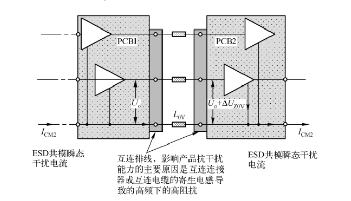
The diagram depicts the conversion principle, where UO represents the normal operating voltage signal transmitted between PCB1 and PCB2.
When no ESD common-mode interference current flows through the flat cable, UO is transmitted from PCB1 to PCB2 without distortion.
However, when the ESD common-mode current flows through the 0V ground path, the inherent parasitic inductance
L (approximately 10 nH/cm) in the interconnections between PCB1 and PCB2 causes the ESD common-mode current to induce a voltage across its two ends. The formula for this induced voltage is as follows:
ΔUZ0V=∣L0V×dICM2/dt∣Assuming the flat cable between PCB1 and PCB2 is approximately 10 cm long, the estimated parasitic inductance is 100 nH. The corresponding induced voltage is calculated as:
ΔUZ0V=∣L×dICM2/dt∣=100 nH×4 A/1 ns=400 VThis induced voltage far exceeds the voltage noise margin of the circuit itself, which is the root cause of the aforementioned system errors.
About Maxipcb
Maxipcb empowers innovators to turn cutting-edge technologies into reality.
We offer one-stop solutions for design, simulation, testing, PCB manufacturing, component procurement and SMT assembly, enabling efficient development, rapid deployment and risk control across the full product lifecycle.Serving the world in communications, industrial automation, aerospace, automotive, semiconductor and beyond, we build a safer, more connected future together.
