In circuit design, it is usually necessary to carry out PCB layout personally. Many professional books detail how to use PCB design software and parameters such as component packages and spacing. Here I summarize my personal experience—some points may be incorrect, and I welcome insights from knowledgeable readers for mutual learning.
Attention to engineers during PCB layout: Component Layout and Soldering Technology
In circuit design, it is usually necessary to carry out PCB layout personally. Many professional books detail how to use PCB design software and parameters such as component packages and spacing. Here I summarize my personal experience—some points may be incorrect, and I welcome insights from knowledgeable readers for mutual learning.
For PCB design software, I use ALTIUM, the one with the most tutorials available. I will not discuss software operations here, but first summarize some useful knowledge before layout: PCBA soldering technology.
Classified by soldering method, there are reflow soldering and wave soldering [Insert Figure: Comparison diagram of reflow soldering and wave soldering]. The simple differences between the two are as follows:
- Reflow soldering can only solder surface mount devices (SMDs). Solder paste is stenciled onto the pads through a steel mesh, then components are placed on the pads, followed by passing through a reflow oven (this oven mainly has several temperature-controlled zones and does not require rosin or molten tin supply). Wave soldering can solder both through-hole components and SMDs; SMDs are generally fixed on the bottom with red glue, through-hole components are inserted from the top, then the board passes through a wave soldering machine (molten tin in the machine surges upward to form numerous tin waves, hence the name "wave soldering").
- Reflow soldering features high precision, allowing dense pad layout; wave soldering has low precision, with component pins prone to short circuits or cold solders, so pad density should be kept low.
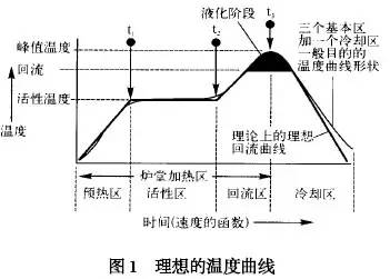 Reflow Oven
 (equipped with four zones of different temperatures inside)
Key parameters: Peak Temperature, Reflow Phase, Liquefaction Phase, Temperature Profile Shape
Basic structure: Three core zones plus one cooling zone
Temperature curve phases: Preheating Zone, Activation Zone, Reflow Zone, Cooling Zone (Time as a function of conveyor speed)
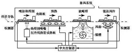
Core components: Air supply system, Conveyor Rails, Flux Sprayer, Circuit Board, Wave Soldering Area, Forced Air Cooling
Auxiliary components: Detector, Infrared Heat Pipe/Hot Plate, Flux Nozzle, Fan, Tin Bath, Central Controller
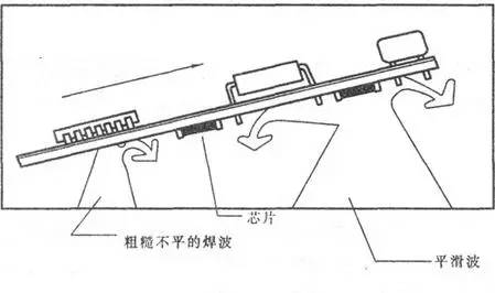
Tin wave types: Rough Uneven Tin Wave, Smooth Tin Wave
After understanding the differences between the two soldering methods, PCB layout must be designed with the intended production process in mind:
- If the board only uses SMDs, reflow soldering is the choice, and it is best to place all components on the same side to complete soldering in a single reflow process.
- If the board includes both SMDs and through-hole components with low pad density, wave soldering is suitable.
Take general household appliance PCBA as an example: They are usually single-layer PCBs. In the past, all through-hole components were used with wave soldering; now, most designs use SMDs on the bottom and through-hole components on the top, then process with wave soldering. This design can reduce the overall PCB area, lower BOM costs (SMD resistors of the same specification are cheaper than through-hole resistors), and often improve product performance.
Recommendations for layout and soldering selection:
- Prioritize the use of SMDs as much as possible.
- If no through-hole components are used: Adopt reflow soldering and place all components on the same side of the PCB.
- If both SMDs and through-hole components are used: Adopt wave soldering, place SMDs on the bottom and through-hole components on the top.
- Design the PCB as a single-layer board if feasible— the cost of a single-layer board is roughly more than half lower than that of a double-layer board.
This is why the PCBs inside most household appliances you disassemble are single-layer boards with through-hole components; the latest designs may be single-layer boards with through-hole components on the top and SMDs on the bottom.
About Maxipcb
Maxipcb empowers innovators to turn cutting-edge technologies into reality.
We offer one-stop solutions for design, simulation, testing, PCB manufacturing, component procurement and SMT assembly, enabling efficient development, rapid deployment and risk control across the full product lifecycle.Serving the world in communications, industrial automation, aerospace, automotive, semiconductor and beyond, we build a safer, more connected future together.

 Reflow Oven (equipped with four zones of different temperatures inside)
Key parameters: Peak Temperature, Reflow Phase, Liquefaction Phase, Temperature Profile Shape
Basic structure: Three core zones plus one cooling zone
Temperature curve phases: Preheating Zone, Activation Zone, Reflow Zone, Cooling Zone (Time as a function of conveyor speed)
Reflow Oven (equipped with four zones of different temperatures inside)
Key parameters: Peak Temperature, Reflow Phase, Liquefaction Phase, Temperature Profile Shape
Basic structure: Three core zones plus one cooling zone
Temperature curve phases: Preheating Zone, Activation Zone, Reflow Zone, Cooling Zone (Time as a function of conveyor speed) Core components: Air supply system, Conveyor Rails, Flux Sprayer, Circuit Board, Wave Soldering Area, Forced Air Cooling
Auxiliary components: Detector, Infrared Heat Pipe/Hot Plate, Flux Nozzle, Fan, Tin Bath, Central Controller
Core components: Air supply system, Conveyor Rails, Flux Sprayer, Circuit Board, Wave Soldering Area, Forced Air Cooling
Auxiliary components: Detector, Infrared Heat Pipe/Hot Plate, Flux Nozzle, Fan, Tin Bath, Central Controller Tin wave types: Rough Uneven Tin Wave, Smooth Tin Wave