Most hidden failures during the mass‑production phase of ICs are not caused by damage to the chip itself, but rather by reliability failures in the board‑level interconnect structures after PCB assembly. AOI, ICT, and power‑on functional testing can only verify that the board powers up correctly at the moment of test;
Most hidden failures during the mass‑production phase of ICs are not caused by damage to the chip itself, but rather by reliability failures in the board‑level interconnect structures after PCB assembly. AOI, ICT, and power‑on functional testing can only verify that the board powers up correctly at the moment of test; they cannot detect latent defects such as solder‑joint thermal fatigue, CTE mismatch, or assembly‑induced bending stress. In automotive electronics applications, solder joints between the IC and PCB are subjected to long‑term exposure to vibration, temperature extremes, and thermal cycling, making them highly susceptible to fatigue and cracking, which can lead to failures. Board‑Level Reliability (BLR) testing is the standardised verification method specifically designed to address these risks.
The industry has established a mature, tiered qualification standard system for automotive applications:
-
AEC‑Q007 – The fundamental board‑level reliability standard dedicated to automotive electronics. It defines the complete BLR testing methodology, graded daisy‑chain design, failure criteria, and statistical analysis. For multi‑chip module (MCM) products, AEC‑Q007 verification must be performed in conjunction with AEC‑Q104.
-
IPC Series Standards – IPC‑9701, IPC‑9702, and IPC‑9703 are general PCB solder‑joint mechanical/thermal stress test standards.
Together, these three categories of standards form the complete board‑level reliability verification framework for automotive ICs, and they are also the core qualification criteria for mass‑production release of consumer, industrial, and automotive products.
Daisy Chain – The Core Vehicle for BLR Testing
The daisy chain forms a conductive path by serially connecting critical interconnect points (such as solder joints, wire bonds, and bumps) of the component. It converts invisible hidden failures – such as micro‑cracks in interconnects, cold solder joints, and pad peeling – into electrical resistance signals that can be captured in real time for quantitative analysis. This is the standard test structure specified by AEC‑Q007.
Based on the failure level being evaluated, the standard divides daisy chains into four grades. Different package types require matching grade‑level designs to precisely locate the failure site.
Daisy‑Chain Selection for Different Package Types
-
Lead‑Frame‑Based Packages – Including SO, QFP, QFN, multi‑row QFN, SON, etc.
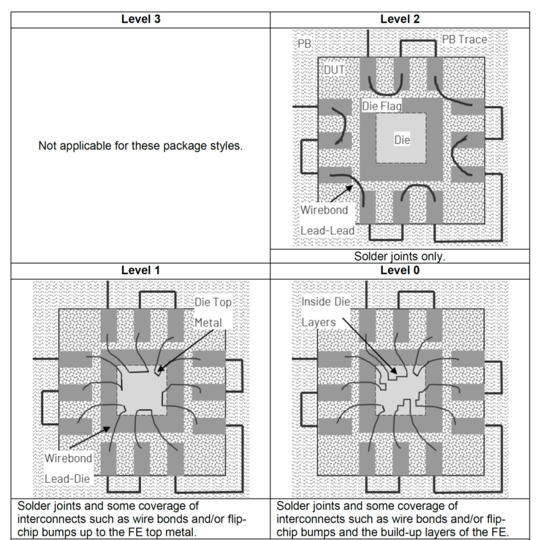
Top view of a package with wire bonds:
-
For solder‑joint and substrate‑trace reliability: choose Level 2.
-
For bond/bump reliability: choose Level 1.
-
For full‑chain reliability: choose Level 0.
-
Substrate‑Based Packages – Including BGA, FCBGA, LGA, FCLGA, etc.
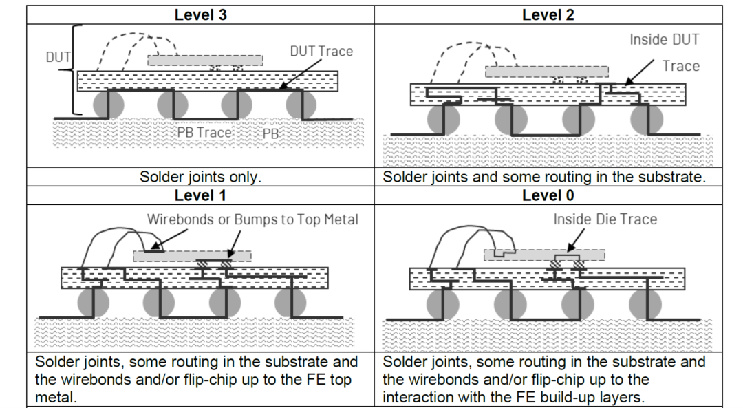
-
For solder‑joint reliability: choose Level 3.
-
For solder‑joint and substrate‑trace reliability: choose Level 2.
-
For bond/bump and chip‑connection reliability: choose Level 1.
-
For full‑chain reliability: choose Level 0.
-
Wafer‑Level Packages – Including WLCSP, FOWLP, etc.
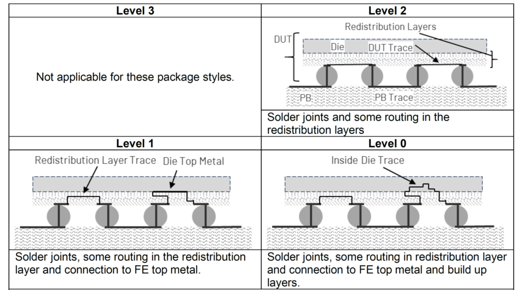
-
For RDL surface‑layer trace reliability: choose Level 2 (including RDL surface traces).
-
For RDL‑to‑chip‑pad connection reliability: choose Level 1 (including the path from RDL to the top metal layer of the chip).
-
For full‑chain reliability: choose Level 0 (including internal chip routing).
PCB Board and Pad Design Guidelines
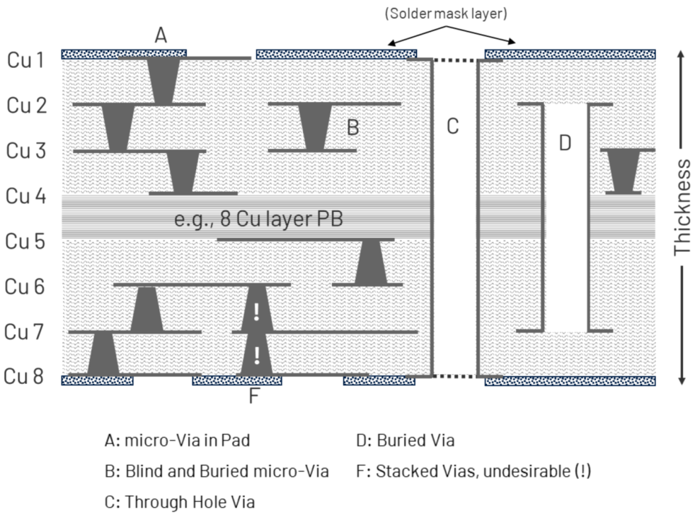
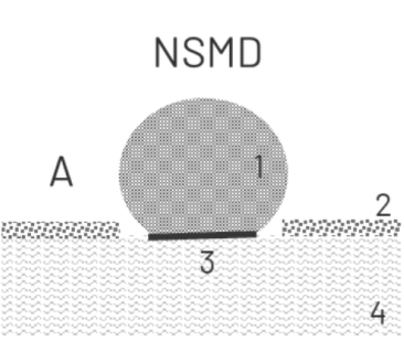
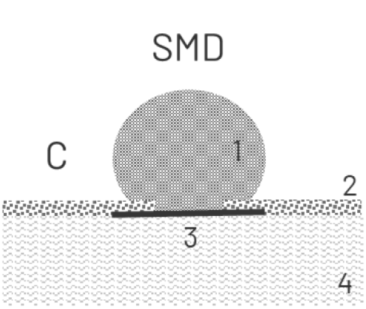
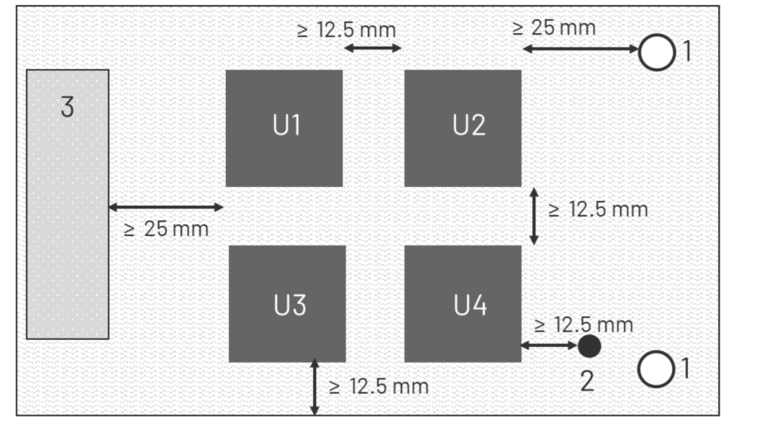
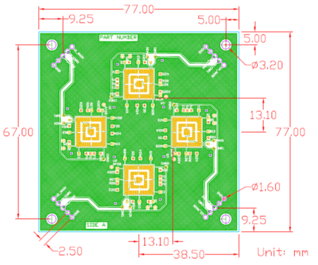
Three Core Board‑Level Reliability Tests
1. Temperature Cycling (TC) Test
Standards: AEC‑Q007‑001, IPC‑9701, JESD22‑A104
Test Procedure:
-
Use an AEC‑Q007‑graded daisy‑chain test board. Measure the initial resistance of each channel using the four‑wire method, and document solder‑joint appearance and X‑ray void data.
-
Place the test boards in an oven with proper support, ensuring uniform temperature change across the entire board area.
-
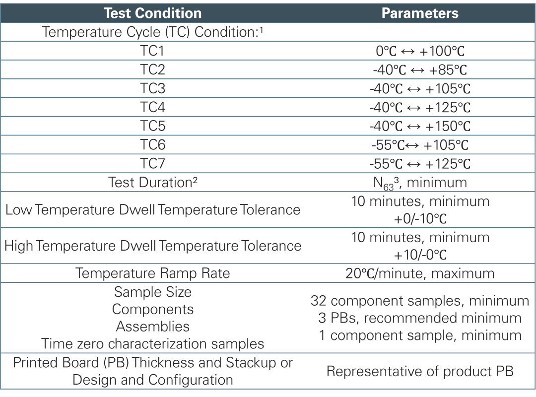
Temperature cycling parameters:
-
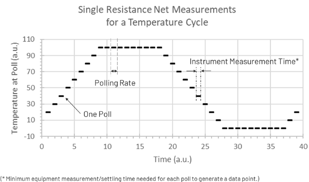
Continuously monitor resistance in real time using a data logger (with data collection at intervals of ≤1 minute). A transient‑interruption monitor may also be used.
-
After the test, allow the boards to recover at room temperature for 2 hours. Perform visual inspection, full‑board X‑ray scanning, and solder‑joint metallographic cross‑section analysis. Perform Weibull life fitting as required by AEC‑Q007.
-
For routine testing, additional samples may be sectioned and analysed at 1000, 1500, 2000, and 3000 cycle intervals.
Acceptance Criteria:
-
Event logger: If the daisy‑chain channel exceeds 1000 Ω for more than 1 μs, and this occurs up to 10 times on the same channel, it is considered a failure.
-
Resistance logger: If the daisy‑chain resistance increase exceeds 20 %, and this occurs up to 5 times on the same channel, it is considered a failure.
2. Mechanical Shock / Drop Test
Standards: IPC‑9703, JESD22‑B111
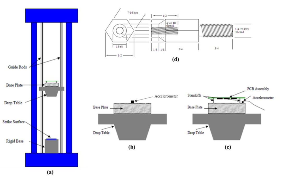
Test Parameters:
-
Half‑sine pulse: 1500 G, 0.5 ms duration.
-
Orientation: –Z direction.
-
Number of drops: Typically 30 drops, or until 50 % to 63 % failure rate is reached.
Acceptance Criteria:
-
Event logger (preferred): If a daisy‑chain channel exceeds 1000 Ω for more than 1 μs, and this same type of transient interruption occurs 3 times within the subsequent 5 test drops on the same channel, it is considered a failure.
-
High‑speed resistance logger (sampling rate ≥ 50 kHz): If the initial daisy‑chain resistance is >85 Ω, and during testing the resistance exceeds 100 Ω or increases by >20 %, and this occurs 3 times within 5 cycles on the same channel, it is considered a failure.
-
If there is no significant resistance increase or intermittent discontinuity, but the component shows visible partial or complete separation from the test board, this should also be considered a failure.
3. Cyclic Bending Test
Standard: JESD22‑B113
Test Procedure:
-
Mount the test board and sample, and attach strain gauges.
-
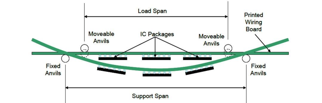
Use two outer support points and two inner loading heads. The components must be positioned in the pure bending region, free from shear stress.
-
Measure deformation and adjust the downward‑stroke test parameters to achieve the specified strain requirements.
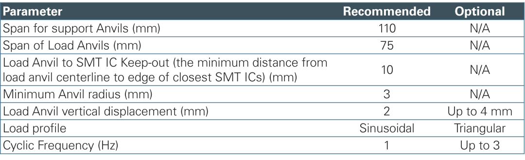
-
Monitor the resistance of all daisy‑chain channels while simultaneously collecting strain data. Record data for at least 10 seconds every 5,000 cycles.
-
The test is typically run until 60 % of the components fail, with an upper limit of 200,000 cycles. If only one board is tested at a time, at least 6 of the 9 SMT ICs on each board should fail (or the test reaches 200,000 cycles) before stopping.
Acceptance Criteria:
-
Event logger: If the daisy‑chain channel exceeds 1000 Ω or 5 times the initial value for more than 1 μs, and this occurs a total of 9 times within a test interval corresponding to 10 % of the cycle count at which the first anomaly appeared, it is considered a failure.
-
Data logger: Continuous data collection – record at least 100 data points exceeding the limit for failure determination. If this occurs a total of 9 times within a test interval corresponding to 10 % of the cycle count at which the first anomaly appeared, it is considered a failure.
Conclusion
Board‑Level Reliability (BLR) is a core qualification step that distinguishes automotive‑grade ICs from ordinary consumer‑grade chips. Leveraging AEC‑Q007‑graded daisy‑chain designs, combined with standardised PCB test vehicles and the three core tests – temperature cycling, mechanical shock/drop, and cyclic bending – BLR testing covers multi‑level failure risks of solder joints, wire bonds, RDL, and internal chip routing under various complex automotive environments. It is an indispensable verification method for ensuring the long‑term stable operation of automotive electronics and for achieving mass‑production qualification of ICs.
About Maxipcb
Maxipcb empowers innovators to turn cutting-edge technologies into reality.We offer one-stop solutions for design, simulation, testing, PCB manufacturing, component procurement and SMT assembly, enabling efficient development, rapid deployment and risk control across the full product lifecycle.
Serving the world in communications, industrial automation, aerospace, automotive, semiconductor and beyond, we build a safer, more connected future together.
