FPC: the full English name is Flexible Printed Circuit, which refers to flexible printed circuit board, also known as flexible board for short. It is made by forming conductor circuit patterns on the surface of a flexible substrate through photoimaging pattern transfer and etching processes.
I. Concept of FPC
FPC: the full English name is Flexible Printed Circuit, which refers to flexible printed circuit board, also known as flexible board for short. It is made by forming conductor circuit patterns on the surface of a flexible substrate through photoimaging pattern transfer and etching processes. The outer and inner layers of double-sided and multi-layer circuit boards realize electrical connection through metalized vias, and the surface of the circuit pattern is protected and insulated by PI (Polyimide) and adhesive layers.
It features high wiring density, light weight and thin thickness, and is mainly used in many products such as mobile phones, laptops, PDAs, digital cameras and LCMs.
II. Main Raw Materials of FPC
Its main raw materials include: 1. Substrate, 2. Coverlay, 3. Stiffener, 4. Other auxiliary materials.
1. Substrate
1.1 Adhesive-backed Substrate
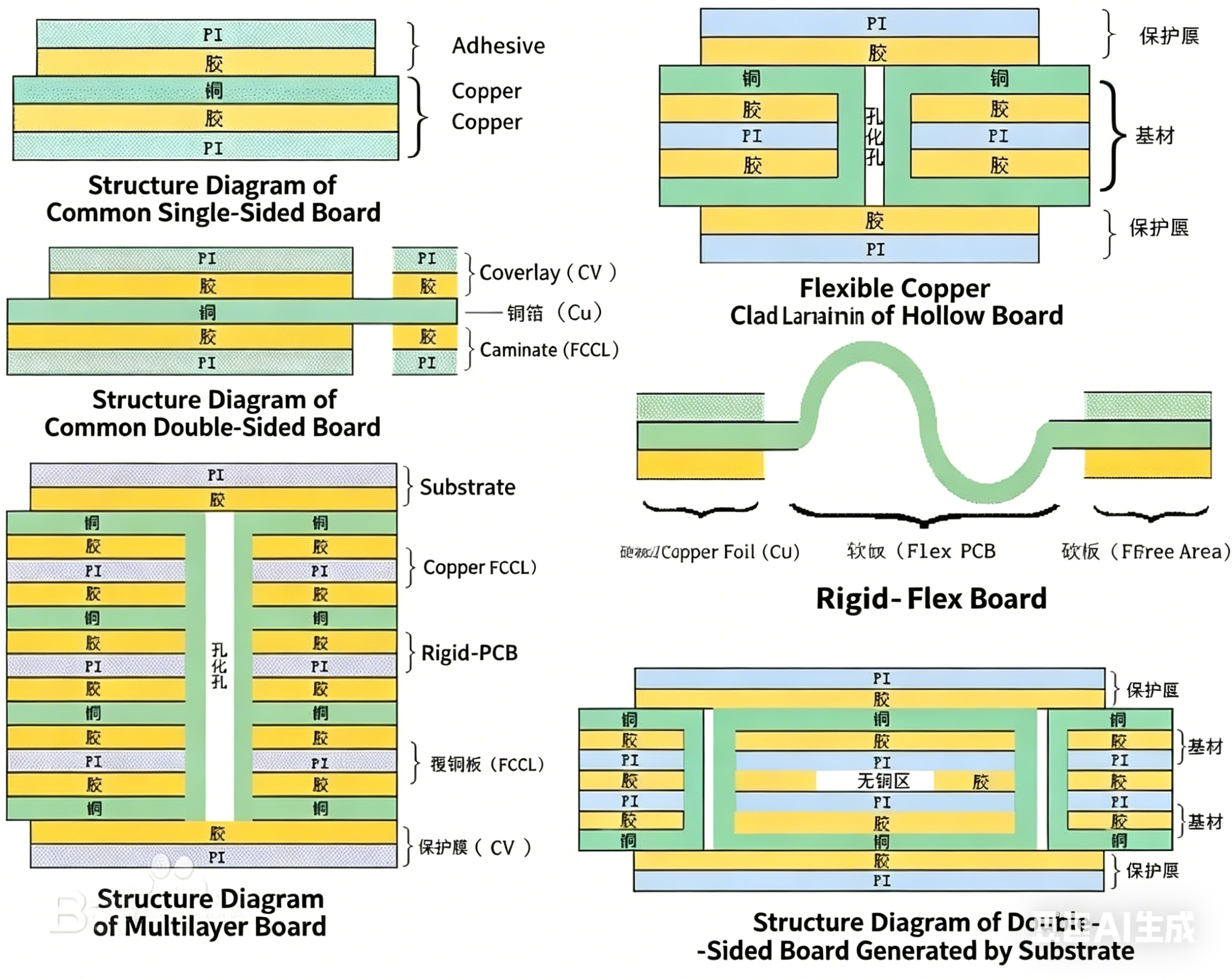
The adhesive-backed substrate is mainly composed of three parts: copper foil, adhesive and PI. It is divided into single-sided and double-sided substrates. The material with copper foil on only one side is a single-sided substrate, and the one with copper foil on both sides is a double-sided substrate.
1.2 Adhesive-free Substrate
The adhesive-free substrate is a substrate without an adhesive layer. Compared with the ordinary adhesive-backed substrate, it lacks the middle adhesive layer and only consists of copper foil and PI. It has the advantages of being thinner, better dimensional stability, higher heat resistance, higher flex resistance and better chemical resistance, and is now widely used.
Copper foil: The commonly used copper foil thickness specifications at present are 1OZ, 1/2OZ and 1/3OZ. A thinner copper foil with a thickness of 1/4OZ has been launched, which is already in use in China for manufacturing ultra-fine line products (line width and spacing of 0.05mm and below). With the increasingly high requirements of customers, this specification of material will be widely used in the future.
2. Coverlay
It is mainly composed of three parts: release paper, adhesive and PI. Only the adhesive and PI remain on the final product, and the release paper is torn off and no longer used during the production process (its function is to prevent foreign matters from adhering to the adhesive).
3. Stiffener
It is a special material for FPC, used in specific parts of the product to increase support strength and make up for the relatively "soft" characteristic of FPC.
The commonly used stiffener materials at present are as follows:
- FR4 stiffener: mainly composed of glass fiber cloth and epoxy resin adhesive, the same as the FR4 material used for PCB;
- Steel sheet stiffener: composed of steel, with high hardness and support strength;
- PI stiffener: the same as the coverlay, composed of PI, adhesive and release paper, but its PI layer is thicker, which can be produced with a thickness ratio from 2MIL to 9MIL.
4. Other Auxiliary Materials
- Pure adhesive film: This bonding adhesive film is a thermosetting acrylate-based bonding adhesive film composed of protective paper/release film and a layer of adhesive. It is mainly used for layered boards, rigid-flex boards and FR-4/steel sheet stiffened boards to play a bonding role.
- Electromagnetic protective film: pasted on the board surface to play a shielding role.
- Pure copper foil: composed of only copper foil, mainly used for the production of hollowed boards.
III. Basic Structure
Copper Foil Substrate:
Copper foil: basically divided into electrolytic copper and rolled copper. The common thicknesses are 1oz, 1/2oz and 1/3oz.
Substrate film: the common thicknesses are 1mil and 1/2mil.
Adhesive (binder): the thickness is determined according to customer requirements.
Coverlay Protective Film:
Coverlay protective film: used for surface insulation, with common thicknesses of 1mil and 1/2mil.
Adhesive (binder): the thickness is determined according to customer requirements.
Release paper: prevents the binder from adhering to foreign matters before lamination and facilitates operation.
Stiffener (PI Stiffener Film):
Stiffener: reinforces the mechanical strength of FPC and facilitates surface mounting operation, with common thicknesses from 3mil to 9mil.
Adhesive (binder): the thickness is determined according to customer requirements.
Release paper: prevents the binder from adhering to foreign matters before lamination.
EMI (Electromagnetic Interference) Shielding Film: protects the circuits inside the circuit board from external interference (strong electromagnetic areas or interference-prone areas).
IV. Characteristics, Advantages and Disadvantages of Flexible Printed Circuits
Core Characteristics
- Short: Short assembly man-hour
All circuits are pre-configured, eliminating the need for additional cable connection work;
- Small: Smaller volume than rigid PCB
It can effectively reduce the product volume and increase portability;
- Light: Lighter weight than rigid PCB
It can reduce the weight of the final product;
- Thin: Thinner than rigid PCB
It can improve flexibility and enhance three-dimensional assembly in limited space.
Advantages of Flexible Printed Circuits
Flexible printed circuits are printed circuits made of flexible insulating substrates, with many advantages that rigid printed circuits do not have:
- It can be freely bent, wound and folded, arranged arbitrarily according to space layout requirements, and moved and stretched arbitrarily in three-dimensional space, thus realizing the integration of component assembly and wire connection;
- The use of FPC can greatly reduce the volume and weight of electronic products, meeting the needs of electronic products developing towards high density, miniaturization and high reliability. Therefore, FPC is widely used in aerospace, military, mobile communication, laptops, computer peripherals, PDAs, digital cameras and other fields or products;
- FPC also has the advantages of good heat dissipation, solderability, easy assembly and low comprehensive cost. The rigid-flex design also makes up for the slight insufficiency of flexible substrates in component bearing capacity to a certain extent.
Disadvantages of Flexible Printed Circuits
- High one-time initial cost: Since flexible PCBs are designed and manufactured for special applications, the initial costs for circuit design, wiring and photomasks are relatively high. Unless there is a special need to use flexible PCBs, it is better not to adopt them for small-quantity applications;
- Difficult modification and repair of flexible PCBs: Once a flexible PCB is manufactured, any modification must start from the base map or compiled photoplotting program, so it is not easy to modify. Its surface is covered with a protective film, which needs to be removed before repair and restored after repair, which is a relatively difficult work;
- Limited size: When flexible PCBs are not yet popular, they are usually manufactured by batch processes, so they are limited by the size of production equipment and cannot be made very long or wide;
- Easy to damage due to improper operation: Improper operation by assembly personnel can easily cause damage to flexible circuits, and its soldering and rework require trained personnel to operate.
V. Types of FPC
Common Types
- Single-sided flexible (IPC-6013 Type 1): A coverlay (polyimide + adhesive) is bonded to an adhesive-free single-sided FPC core, with or without stiffeners.
- Double-sided flexible (IPC-6013 Type 2): Coverlays are bonded to both sides of an adhesive-free double-sided FPC core (two conductive layers) with plated through-holes, with or without stiffeners.
- Multi-layer flexible (IPC-6013 Type 3): Coverlays are bonded to both sides of an adhesive-free structure containing three or more conductive layers with plated through-holes, with or without stiffeners.
Our current manufacturing capacity for multi-layer Flex PCB is up to 12 layers.
Other Types
- Hollowed board: also known as window board (windowed on the finger side).
- Layered board: with separate circuits on both sides.
- Rigid-flex board: a product combining flexible board and rigid board.
VI. Calculation of Bending Radius of FPC Flexible Boards
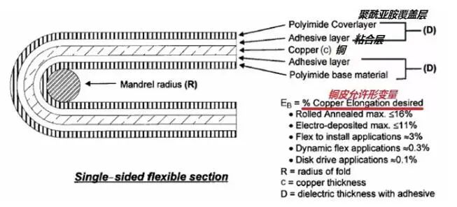
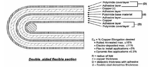
When an FPC flexible circuit board is bent, the types of stress on both sides of its center line are different. The inner side of the bending surface is under pressure, and the outer side is under tension. The magnitude of the stress is related to the thickness and bending radius of the FPC flexible circuit board. Excessive stress will cause delamination, copper foil fracture and other problems of the FPC flexible circuit board. Therefore, in the design, the lamination structure of the FPC flexible circuit board should be reasonably arranged to make the lamination on both ends of the center line of the bending surface as symmetrical as possible. At the same time, the minimum bending radius should be calculated according to different application scenarios.
Calculation Method of Bending Radius of FPC Flexible Boards
Case 1: Minimum bending of single-sided flexible circuit boards
Its minimum bending radius can be calculated by the following formula:
R=(c/2)[(100-Eb)/Eb]-D
Where:
R = minimum bending radius (unit: µm)
c = copper foil thickness (unit: µm)
D = coverlay thickness (unit: µm)
EB = allowable copper foil deformation (measured as a percentage)
Different types of copper have different copper foil deformation values:
A. The maximum allowable deformation of rolled copper foil is ≤16%
B. The maximum allowable deformation of electrolytic copper foil is ≤11%
Moreover, the deformation value of copper foil of the same material is different in different application scenarios:
- For one-time bending occasions, the limit value of the fracture critical state is used (16% for rolled copper);
- For bending installation design, the minimum deformation value specified by IPC-MF-150 is used (10% for rolled copper);
- For dynamic flexible applications, the copper foil deformation is 0.3%;
- For magnetic head applications, the copper foil deformation is 0.1%.
The minimum bending radius can be calculated by setting the allowable deformation of the copper foil.
Dynamic flexibility: This application scenario of copper foil realizes functions through deformation. For example, the phosphor copper shrapnel in the IC card holder is the part that contacts the chip after the IC card is inserted, and the shrapnel deforms continuously during insertion—this application scenario is dynamically flexible.
Case 2: Double-sided boards
Formula for minimum bending radius:
R=(c/2)[(100-Eb)/Eb]-D-d
Where:
R = minimum bending radius (unit: µm)
c = copper foil thickness (unit: µm)
D = coverlay thickness (unit: µm)
EB = copper foil deformation (measured as a percentage, the value is the same as above)
d = interlayer dielectric thickness (unit: µm)
Minimum Bending Radius and Flexural Strength of Flexible Boards
- Single-sided board: 3~6 times the wire thickness
- Double-sided board: 6~10 times the wire thickness
- Multi-layer flexible board: 10~15 times the wire thickness
- Dynamic single-sided board: 20~40 times the wire thickness
VII. FPC Production Process
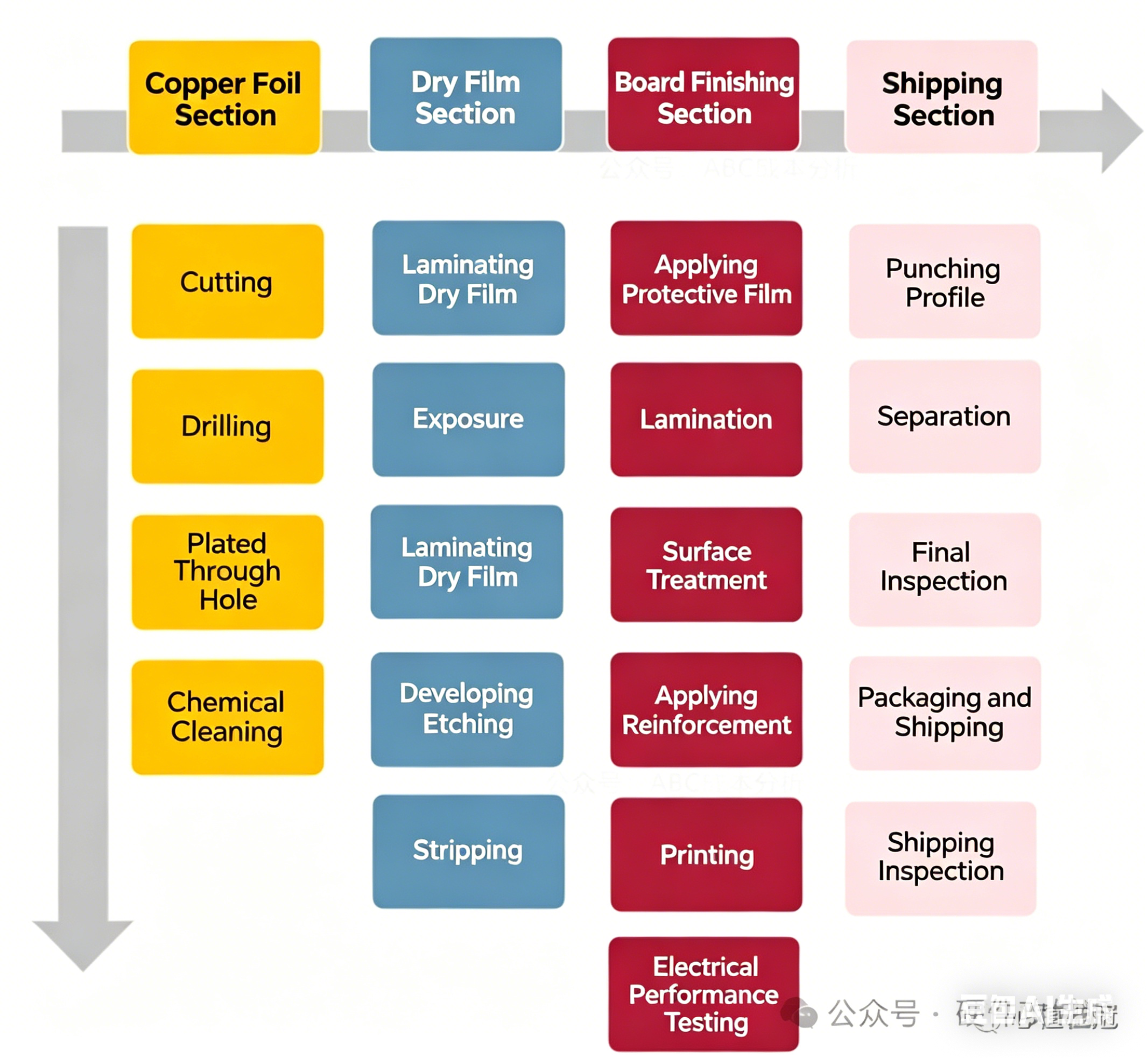
General Process Stages for FPC Single and Double-sided Boards
Detailed Process of Single-sided Board
Material cutting → Baking → Laminating dry film → Exposure → Development → Etching → Stripping → Pre-treatment → Laminating coverlay → Lamination → Curing → Surface treatment → Electrical testing → Assembly → Lamination → Curing → Marking → Blanking → Final inspection → Packaging and shipping
Detailed Process of Double-sided Board
Material cutting → Baking → Drilling → Black hole → VCP → Pre-treatment → Laminating dry film → Exposure → Development → Etching → Stripping → Pre-treatment → Laminating coverlay → Lamination → Curing → Surface treatment → Electrical testing → Assembly → Lamination → Curing → Marking → Blanking → Final inspection → Packaging and shipping
About Maxipcb
Maxipcb empowers innovators to turn cutting-edge technologies into reality.
We offer one-stop solutions for design, simulation, testing, PCB manufacturing, component procurement and SMT assembly, enabling efficient development, rapid deployment and risk control across the full product lifecycle.Serving the world in communications, industrial automation, aerospace, automotive, semiconductor and beyond, we build a safer, more connected future together.