This document shares content from Acceptance Conditions for High-Reliability Printed Circuit Boards in DFM.
This document shares content from Acceptance Conditions for High-Reliability Printed Circuit Boards in DFM.
1. Basic Functions of the Printed Substrate
- Sufficient mechanical strength.
- Withstand thermal treatment and mechanical shock during assembly.
- Sufficient flatness for automated assembly processes.
- Withstand 6 or more soldering and rework cycles.
- Good electrical performance and moisture resistance.
- Excellent dimensional stability.
2. Performance Classes of Printed Circuit Boards
Military-grade PCBs are classified into three classes:
- Class 1: General military electronic equipment (ground and common military devices). Requires complete function, reasonable service life and reliability; minor cosmetic defects that do not affect electrical/mechanical performance are allowed.
- Class 2: Special military electronic equipment (military communications, complex military electronics). Requires complete function, long service life and high reliability; slight cosmetic defects that do not impair performance are allowed.
- Class 3: High‑reliability military electronic equipment (vehicle‑mounted, airborne, shipboard, aerospace). Requires complete function, long service life, continuous operation and ultra‑high reliability; no failures permitted in service.
3. Basic Requirements for Printed Circuit Boards
-
PCBs must comply with design and process documentation. The number of copper-clad layers (single‑sided, double‑sided, multilayer) shall match the board structure and be compatible with components and process materials used in assembly.
-
Appearance Requirements
- Substrate surface shall be flat, with clean edges and undistorted patterns; no cracking, burrs, blisters or delamination.
- Printed conductors shall be smooth and uniform in color; no foil lifting, bulging or obvious scratches.
- Surface plating shall be bright and uniform, without peeling or blistering.
- Solder mask thickness shall not exceed pad thickness.
- Pads shall be free of markings, solder mask or contamination.
- Other properties shall comply with GJB 362B.
-
PCBs shall be compatible with wave soldering and reflow soldering.
-
Flatness (Warpage and Twist)
- Warpage/twist of through‑hole PCBs before soldering: ≤ 1%.
- Warpage/twist of surface‑mount PCBs: generally ≤ 0.75%; for fine pitch: ≤ 0.5%.
-
Process reference holes, identification marks and pad mounting accuracy shall meet assembly requirements. Marks shall be flat, clean, uniformly bright and high‑contrast against the background.
-
Selection of Surface Coating/Plating
- Military PCBs shall use HASL or electrolytic Ni/Au; immersion Ni/Au is not allowed. Plating type shall be marked on the assembly drawing.
- Solderability protection for pads and PTHs: Pb‑Sn alloy with Pb ≥ 3%. SMT pads: Pb‑Sn layer 2.8 μm–8 μm. Class 3 and high‑density PCBs are recommended to use electrolytic Ni/Au: Ni 5 μm–7 μm, Au 0.05 μm–0.15 μm.
- Solder mask application follows GJB 362B 3.5.1.8. Cured solder mask minimum thickness: Class 2 10 μm, Class 3 18 μm (per GJB 4057).
- For areas where shielding cans are screw‑mounted or soldered, minimize Pb‑Sn coating area, or use a crosshatched ground plane design.
-
Solderability
-
Solderability of Plated Through Holes (PTHs)
After testing per QJ832A, solder shall wet the surrounding pads. At
232℃–237℃ for
3 s, the metal plating must fully wet the hole wall; no non‑wetting or exposed base metal. Contact angle <
90°.
-
Surface Solderability (per Table 4)
| Solder Temperature (℃) |
Allowed Soldering Time (s) |
Solder Appearance |
Quality Evaluation |
| 232+5 |
3 |
Full wetting |
Excellent, accepted |
| 232+5 |
5 |
Full wetting |
Good, accepted |
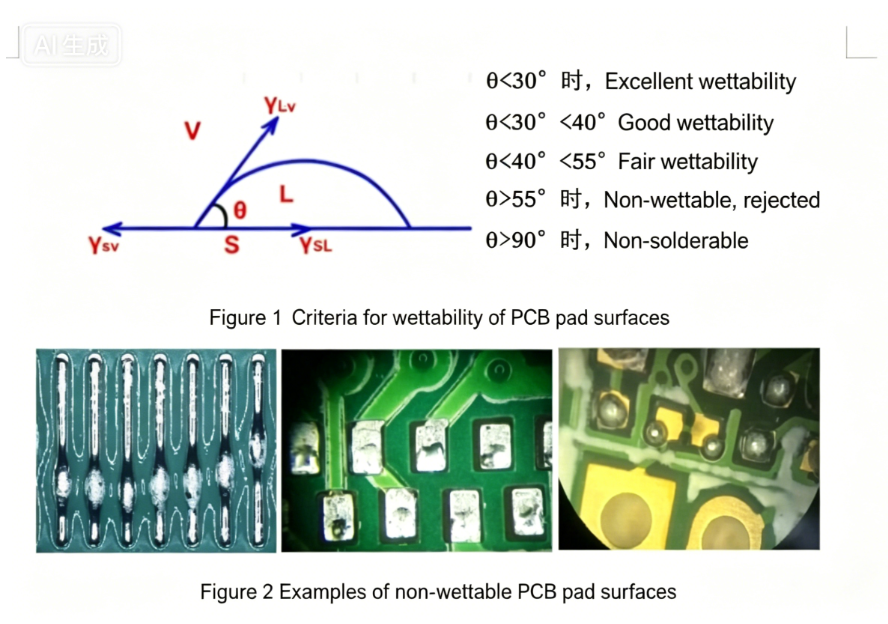
- Wetting criterion:
- θ < 30°: Excellent wetting
- 30° ≤ θ < 40°: Good wetting
- 40° ≤ θ < 55°: Fair wetting
- θ > 55°: Non‑wetting, rejected
- θ > 90°: Unsolderable
-
Heat Resistance (Thermal Stress)
- After dipping in molten solder at 287℃±6℃ for 10 s–11 s, no delamination, blistering or damage; peel strength of outer conductors meets requirements; solder mask shall not wrinkle or peel.
- Process temperatures:
- Manual soldering: 240℃±10℃
- Wave soldering: 250℃±5℃
- Reflow soldering: 235℃±5℃
- Delamination, blistering, damage or solder mask failure under these conditions indicates failed heat resistance.
-
Peel Strength for FR‑4 (Flame‑Retardant Epoxy Glass Cloth)
- Normal conditions:
- Cu thickness ≥ 35 μm: ≥ 1.4 N/mm
- Cu thickness = 18 μm: ≥ 1.1 N/mm
- After environmental testing:
- −65±2℃ for 6 h → 125±2℃ for 16 h → cyclic humidity for 48 h
- Multilayer FR‑4 outer conductors: ≥ 1.2 N/mm
-
Substrate Selection
- Determine thickness based on board size and component weight per unit area.
- Consider electrical performance, Tg, CTE, flatness and metallization capability.
- Unless otherwise specified, use FR‑4 substrate.
4. Mixed‑Technology PCBs
-
Substrate Requirements for Mixed Assemblies
Choose based on performance, environment and soldering temperature:
- < 240℃: Standard FR‑4.
- 240℃–250℃: High‑Tg FR‑4 (Tg 150℃–170℃).
- For products with high reliability, thick plate and welding temperature above 250℃, FR-5 is adopted;
- High temperature or flexible circuits: Polyimide glass cloth.
- High‑reliability, high‑heat dissipation: Metal core substrate.
- High‑frequency circuits: PTFE glass cloth.
-
Pad Surface Plating for Mixed Assemblies
- Plating must meet GJB 362B solderability.
- High‑reliability military: Recommended HASL (Pb‑Sn).
- High flatness required: Recommended electrolytic Ni/Au.
- High‑density assembly: Recommended electrolytic Ni/Au; alternative: HASL.
- Not recommended: A‑side HASL (Pb‑Sn) + B‑side lead‑free coating to avoid component drop during double reflow. Solve by layout or process instead.
-
Design Rules for Double‑Sided Reflow
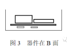
- Place large components on Side A, small components on Side B.
- Component mass / total pad area < 30 g/in² to prevent dropping during second reflow.
-
Process Solutions
- Set a vertical temperature gradient in the reflow oven: bottom zone 20℃–30℃ cooler than top.
- Use adhesive to fix B‑side components before solder paste printing to prevent shifting or falling.
5. Quality Requirements for White Spots, Microcracks, etc.
5.1 IPC‑610E‑213
-
White Spots
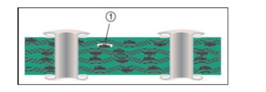
- Definition: Separation of glass fiber and resin at cross‑weave points, visible as white spots or cross patterns under the surface, usually caused by thermal stress.
- Accept
- Class 1/2/3: No white spots (ideal).
- Class 1/2: Allowed if function is normal.
- Class 3: Process alert if area exceeds 50% of conductor spacing.
- Note: White spots are not defects and are not proven to promote CAF.
-
Microcracks
- Definition: Continuous white lines or cross patterns from fiber‑resin separation, usually caused by mechanical stress.
- Accept
- Class 1: Allowed if function is normal.
- Class 2/3: Area ≤ 50% of conductor spacing; does not reduce clearance below minimum.
- Reject (Class 2/3): Area > 50% of spacing; reduces clearance below minimum; edge cracks reduce conductor‑to‑edge distance < 2.5 mm (if not specified).
-
Blisters and Delamination
- Definition:
- Blister: Local expansion and separation between layers or between substrate and foil/coating.
- Delamination: Separation within the laminate or between substrate and foil.
- Accept (Class 1/2/3): Affected area ≤ 25% of PTH/conductor spacing; does not reduce clearance below minimum.
- Reject: Area > 25% of spacing; reduces clearance below minimum.
-
Weave Exposure and Fiber Exposure
- Weave exposure: Acceptable for all classes.
- Fiber exposure:
- Accept: Does not reduce clearance below minimum.
- Reject (Class 2/3): Fiber damage; reduces clearance below minimum.
5.2 IPC‑6012C (2010)
- White Spots: Acceptable for all classes. Process alert for Class 3 if > 50% of spacing.
- Microcracks: Acceptable if no spacing violation and no growth after thermal stress; ≤ 50% of spacing for Class 2/3.
- Delamination/Blisters: Acceptable if ≤ 1% of board area, no spacing violation, no growth; ≤ 25% of spacing for Class 2/3.
5.3 GJB 4896‑2003
- White Spots: Acceptable except for high‑voltage products.
- Microcracks: Accept if no spacing violation, no growth after stress; edge distance > 2.5 mm (if unspecified); ≤ 50% of spacing for Class 2/3.
- Delamination/Blisters: Accept if ≤ 1% of board area, no spacing violation, no growth; ≤ 25% of spacing for Class 2/3.
5.4 GJB 362B‑2009
- Spots: Accept if translucent, weave pattern only, ≥ 0.25 mm from conductors, no growth after soldering.
- White Spots/Cracks: Accept if not for high‑voltage fields; total area ≤ 2% of board; size ≤ 0.80 mm; no bridging; no spacing violation; no growth; edge distance > 2.5 mm (if unspecified); cracks ≤ 50% of spacing.
5.5 QJ 831B‑2011
- White Spots/Cracks: ≤ 2% of board area; ≤ 25% of inner‑layer spacing; size ≤ 0.8 mm (non‑high‑voltage).
- Subsurface Spots: Accept if translucent, weave pattern, ≥ 0.25 mm from conductors, no growth after soldering.
Conclusion
To improve design and assembly quality, DFM and process control are essential. High‑reliability PCBA must follow clear acceptance criteria (e.g., GJB 362B for military products) to control incoming quality.
Most white spots in assembly are caused by
excessively high soldering temperature, insufficient Tg, or long soldering time. Prevention through design and process control is far more effective than post‑failure analysis.
About Maxipcb
Maxipcb empowers innovators to turn cutting-edge technologies into reality.
We offer one-stop solutions for design, simulation, testing, PCB manufacturing, component procurement and SMT assembly, enabling efficient development, rapid deployment and risk control across the full product lifecycle.Serving the world in communications, industrial automation, aerospace, automotive, semiconductor and beyond, we build a safer, more connected future together.