RF antenna plays a vital role in the performance of wireless communication systems. Its efficiency directly impacts signal strength, data transmission quality, and overall system reliability. In the context of PCB design and manufacturing, the integration of an RF antenna PCB involves much more than simply placing it on the board—it requires precise design, high-performance materials, and stable manufacturing processes to ensure consistent functionality across environments. With the rapid growth of technologies like 5G, Wi-Fi, Bluetooth, and IoT, optimizing antenna performance has become a central task for PCB engineers.
RF antenna layout begins at the earliest stages of PCB design. Since the antenna is typically located at the end of the RF signal path, its placement must account for isolation from noise sources, minimal obstruction, and proper ground referencing. For example, in 2.4 GHz applications, common antenna types like inverted-F (IFA), meandered monopole, and patch antennas must be designed with trace lengths and geometry tuned to resonate at the desired frequency. Simulation tools such as HFSS, ADS, or CST are widely used by engineers to match the antenna’s impedance to 50 ohms and ensure optimal radiation patterns. Careful control of line width, clearance to ground, and antenna orientation all contribute to achieving stable performance.
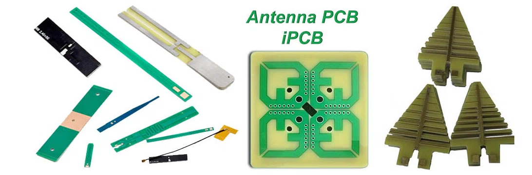
RF antenna
RF antenna performance is highly dependent on the stack-up and materials used in PCB fabrication. Standard FR4 materials, though economical, exhibit higher signal loss at frequencies above 1 GHz, making them unsuitable for critical RF applications. Instead, designers often opt for high-frequency laminates like Rogers RO4350B, RO4003C, or PTFE-based materials, which offer lower dielectric constants and loss tangents. These substrates support better signal integrity and allow finer trace control. Layer stack-up choices must also consider the spacing between the RF layer and ground planes to maintain consistent impedance and reduce parasitic effects. Manufacturing tolerances in trace width, dielectric thickness, and copper roughness all directly impact antenna behavior, which is why many RF boards undergo tight process control and impedance verification testing.
Antenna PCB fabrication also requires strict attention to detail during production. Burrs or imperfections introduced during etching can degrade radiation efficiency or shift resonance frequency. The use of surface finishes like ENIG (Electroless Nickel Immersion Gold) or silver plating is common in antenna regions to ensure low surface resistance and stable contact. When using via-in-pad or coplanar waveguide structures, proper solder mask clearance and via design are essential to minimize signal loss. Manufacturers may employ X-ray or TDR (Time Domain Reflectometry) tools to assess the physical and electrical quality of antenna traces. In multilayer designs, maintaining isolation between RF and digital circuits with grounded guard traces or stitching vias is also critical to prevent coupling or crosstalk.
RF antenna design must also consider environmental and mechanical factors. Nearby components such as LCDs, batteries, or enclosures can significantly affect antenna tuning and efficiency. For instance, metallic cases or proximity to ground planes may cause detuning or reduce gain. This makes 3D simulation and prototype testing essential to validate antenna performance in its final assembly. In compact devices like smartwatches, earbuds, or IoT sensors, chip antennas or embedded PCB antennas are often used due to space constraints, but they demand extremely precise layout control. Matching networks, placed close to the feed point, are fine -tuned during development using vector network analyzers (VNAs) to reduce return loss and maximize power transfer.
RF antenna optimization in PCB design is essential for modern wireless products, especially as applications demand higher frequency, smaller size, and greater integration. The evolution toward millimeter-wave communication, phased-array antennas, and beamforming systems presents new challenges that require advanced PCB materials, tighter process tolerances, and closer collaboration between RF engineers and board fabricators. With growing emphasis on EMC compliance and energy efficiency, antenna design is no longer a standalone task—it is an integrated effort tied to the entire PCB system. By addressing layout, material, fabrication, and environmental interaction in unison, engineers can deliver antenna solutions that meet the demands of the next generation of wireless technologies.


