The selection of PCB board connectors is a core decision-making link in the early stage of PCB design, requiring comprehensive evaluation based on three aspects: circuit function requirements, PCB physical characteristics, and application environment. From the perspective of circuit functions, the current-carrying capacity, signal transmission rate, and impedance matching characteristics of the connector must be highly aligned with the circuit topology of the PCB to avoid local heating caused by excessive resistance. In terms of PCB physical characteristics, the connector’s package type and pin pitch must be compatible with the PCB’s size, number of layers, and wiring density. The application environment is also a non-negligible factor in selection: in the consumer electronics field, PCB board connectors need to meet the demands of miniaturization and low cost while having a certain ability to resist temperature and humidity changes.
The layout design of PCB board connectors directly affects the signal transmission quality and production efficiency of the PCB, and must follow the principle of "signal priority, with process considerations". From the perspective of signal integrity, the connector layout should minimize parasitic parameters and interference in the signal path. Secondly, different types of connectors need to be laid out in separate zones to avoid interference. For example, radio frequency (RF) connectors (such as SMA interfaces) should be placed independently in a "clean area" of the PCB, away from digital circuits (e.g., CPUs, memory), and isolated by a ground plane to reduce the impact of digital noise on RF signals. From the perspective of production feasibility, the connector layout must be compatible with PCB manufacturing and assembly processes. Connectors should be avoided in PCB corners or too close to edges (typically at least 2mm away from the PCB edge) to prevent damage during PCB cutting or poor alignment with external devices during assembly.
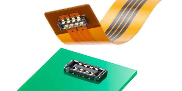
PCB board connectors
The reliability of PCB board connectors depends on process adaptability throughout the entire PCB production flow, from substrate material selection and pad processing to soldering inspection—each step requires strict control. In substrate material selection, the PCB substrate must have sufficient mechanical strength and thermal stability to withstand the connector’s insertion/extraction force and operating temperature rise.Pad processing is critical to ensuring connector soldering quality. Common pad plating processes include HASL, ENIG, and (ImAg. HASL is low-cost but has poor surface flatness, making it suitable for connectors with larger pin pitches (≥1.0mm). ENIG offers flat surfaces, high soldering reliability, and excellent oxidation resistance, making it ideal for high-density connectors with small pin pitches (≤0.5mm), though it is more expensive. Immersion Silver balances cost and reliability, making it suitable for PCB board connectors in mass-produced consumer electronics.
In the PCB design and production of different industries, the selection, layout, and process adaptability of PCB board connectors show significant differences, driven by each industry’s unique demands for performance, reliability, and cost. In consumer electronics, for example, connectors for smartphone PCBs need to meet miniaturization and high-density requirements. In automotive electronics, on-board PCBs have extremely high reliability requirements for connectors—for instance, the connection between an ADAS (Advanced Driver Assistance Systems) PCB and a camera module uses automotive-grade board-to-board connectors. In industrial control, connectors for PLC PCBs must balance reliability and maintainability.
In summary, PCB board connectors, as critical linking components in PCB design and production, are deeply tied to application scenarios through their selection, layout, and process adaptability—directly influencing the performance, reliability, and cost of electronic systems. As electronic technology advances toward miniaturization, higher speed, and greater reliability, PCB board connectors will face more stringent requirements, such as higher signal transmission rates (≥20Gbps), larger current-carrying capacities (≥100A), and stronger environmental tolerance. Only by continuously integrating circuit design theory, materials science, and manufacturing processes can the application of PCB board connectors be optimized, providing more reliable "linkage guarantees" for PCB design and production, and driving electronic devices toward higher performance, greater stability, and better cost-effectiveness.


