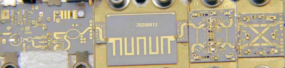
• Microwave circuit PCB
  • Microwave circuit PCB
  • Microwave circuit PCB
  • Microwave circuit PCB

Microwave circuit PCB

Product Model: Microwave Circuit PCB
Material: Teflon, PTFE, Ceramic
Quality Standard: IPC 6012 Class 2
Dielectric Constant (DK): 1.6 - 2.0
Layer Count: 1–36 layers
Board Thickness: 0.254mm - 12mm
Base Copper Weight: 0.5oz / 1oz
Surface Finish: Silver, Gold, OSP
Special Process: Mixed material lamination, stepped groove processing
Application: Microstrip antenna, radar PCB

  • Microwave circuit PCB
  • Microwave circuit PCB
  • Description

  • Data Sheet

1. Overview of Microwave Circuit PCB

Microwave Circuit PCB is a specialized printed circuit board designed for high-frequency signal transmission, with an operating frequency range typically between 300MHz and 300GHz. It is widely applied in communication, radar, radio and other high-frequency fields, featuring excellent high-frequency performance, compact structure and high operational reliability. As the core carrier of microwave signal transmission, it plays a crucial role in ensuring the stability and efficiency of high-frequency equipment.
A microwave circuit refers to a functional circuit operating in the microwave and millimeter-wave bands, integrated on a substrate with microwave passive components, active components, transmission lines and interconnection structures. Its core function is to realize the generation, amplification, transmission and processing of high-frequency signals, which is the key to the normal operation of microwave equipment.

2. Classification of Microwave Circuits

Microwave circuits are mainly divided into two categories: Hybrid Microwave Integrated Circuit (HMIC) and Monolithic Microwave Integrated Circuit (MMIC), which differ in structure, manufacturing process and application scenarios.

2.1 Hybrid Microwave Integrated Circuit (HMIC)

HMIC is a functional module fabricated by depositing passive microwave circuits on a microwave-compatible substrate using thin-film or thick-film technology, and then assembling discrete active components at designated positions. It is custom-designed and manufactured according to system requirements, with strong flexibility in structure and process.
The substrates used in HMIC include high-alumina ceramics, sapphire, quartz, high-performance ceramics and organic media, which have excellent high-frequency electrical properties and thermal stability. The circuit forms are divided into distributed parameter microstrip circuits and lumped parameter circuits; active components can adopt packaged microwave devices or bare chips. The core feature of HMIC is that it is designed for specific microwave equipment and frequency bands, with strong specificity. Common HMIC products include microstrip mixers, microwave low-noise amplifiers, power amplifiers, frequency multipliers, phased array units and various broadband microwave modules.

2.2 Monolithic Microwave Integrated Circuit (MMIC)

MMIC is an integrated circuit that integrates microwave functional circuits (components, transmission lines, interconnection lines) on a semiconductor substrate through semiconductor manufacturing processes. Gallium Arsenide (GaAs) is the most commonly used substrate material; microwave circuits fabricated on silicon substrates, which operate in the 300GHz-3000GHz frequency band, are classified as extensions of silicon linear integrated circuits and not included in the scope of MMIC.
The manufacturing process of GaAs MMIC mainly includes the following steps: forming an active layer on a semi-insulating GaAs wafer through epitaxial growth or silicon ion implantation; implanting oxygen, protons or other appropriate ions to form an isolation layer; implanting beryllium or zinc to form PN junctions; preparing metal-semiconductor barriers by electron beam evaporation; and fabricating active devices (diodes, field-effect transistors), passive components (inductors, capacitors, resistors, microstrip couplers, filters, loads) and circuit patterns. MMIC design is divided into lumped parameter and distributed parameter forms, among which distributed parameters are mainly used in power circuits and millimeter-wave circuits (operating frequency range: 30GHz-300GHz).
GaAs is more suitable for manufacturing MMIC (including ultra-high-speed circuits) than silicon, mainly due to three advantages: first, the resistivity of semi-insulating GaAs substrate is as high as 10⁷~10⁹ Ω·cm, which effectively reduces microwave transmission loss; second, the electron mobility of GaAs is about 5 times that of silicon, enabling higher operating frequency and faster signal transmission speed; third, the key active device GaAs metal-semiconductor field-effect transistor (MESFET) is a multi-functional device with excellent radiation resistance. Therefore, GaAs MMIC has broad application prospects in solid-state phased array radars, electronic countermeasure equipment, tactical missiles, TV satellite reception, microwave communications, ultra-high-speed computers and large-capacity information processing systems.
Currently, mature MMIC products that have been developed and applied include monolithic microwave integrated low-noise amplifiers, monolithic TV satellite receiver front-ends, monolithic microwave power amplifiers and monolithic microwave voltage-controlled oscillators. MMIC design focuses on the generation, amplification, control and information processing of microwave signals, with strong specificity for different equipment and frequency bands.


Microwave circuit PCB


3. Material Selection and Design of Microwave Circuit PCB

Material selection and structural design are the core links to ensure the stable operation of microwave circuit PCB under high-frequency conditions. Scientific material selection and reasonable structural design can significantly improve signal transmission efficiency and equipment reliability.

3.1 Material Characteristics

Microwave circuit PCB materials must have specific electrical properties, mainly including dielectric constant (Dk) and dielectric loss factor (Df). Dielectric constant reflects the ability of a material to store electrical energy, while dielectric loss factor characterizes the energy loss converted into heat during signal transmission. In high-frequency applications, materials with low and stable Dk and Df are preferred, which can minimize signal loss and ensure the integrity of high-frequency signal transmission.

3.2 RF Material Selection

When selecting microwave circuit PCB materials, factors such as environmental humidity, thermal stability and chemical resistance must be comprehensively considered to ensure reliable performance under various operating conditions. Commonly used microwave circuit PCB materials include FR-4, Polytetrafluoroethylene (PTFE) and ceramic materials. Among them, PTFE has excellent high-frequency characteristics (low Dk, low Df, stable electrical properties), making it widely used in high-performance microwave applications that require strict signal integrity.

3.3 Design Structure

The common structural forms of microwave circuit PCB include microstrip lines and striplines. A microstrip line is composed of a conductive strip on a dielectric substrate and a ground plane under the substrate, which is suitable for high-frequency signal transmission and has the advantages of simple structure and easy processing. A stripline is composed of a conductive strip clamped between two ground planes, which provides better electromagnetic shielding performance and is suitable for applications with high requirements for signal integrity and anti-interference ability.

3.4 Impedance Matching

Impedance matching is a key link in microwave circuit PCB design, which directly affects signal integrity. Good impedance matching can reduce signal reflection, optimize power transmission efficiency and avoid signal distortion. In the design process, it is necessary to reasonably design the layout of transmission lines and select appropriate substrate materials, and often use electromagnetic simulation technology for analysis and adjustment to ensure that the impedance meets the design requirements.

3.5 Thermal Design

High-power components on microwave circuit PCB will generate a lot of heat during operation, so reasonable thermal design is crucial to ensure the long-term stable operation of equipment. Common thermal design measures include optimizing the layout of high-power components to enhance thermal contact, using thermal vias to improve temperature uniformity, and selecting substrate materials with good thermal conductivity to accelerate heat dissipation.

 Microwave circuit PCB

4. Development History and Current Status of Microwave Circuits

4.1 Development History

The concept of microwave circuits originated in the 1930s, when waveguides were recognized as an effective transmission structure for microwave frequencies. After appropriate modification, short waveguide segments can be used as radiators or resonant components (such as resonant cavities and horn antennas). In the early stage of development, the core demand was to realize the effective transmission and recovery of microwave power between microwave sources, transmission lines and receivers, which promoted the emergence of traveling wave detectors, wavelength meters, terminal loads and other components.
Microwave circuit technology officially took off in the 1950s. The development of microwave solid-state devices promoted the transformation of microwave circuit technology from coaxial lines, waveguide components and their systems to planar circuits. In the 1960s and 1970s, alumina substrates and thick-film technology were widely used in microwave circuit manufacturing; in the 1980s, monolithic microwave integrated circuits began to emerge and gradually enter the practical stage. In 1974, Plessey of the United States successfully developed the world's first MMIC amplifier using GaAs FETs as active devices and GaAs semi-insulating substrates as carriers, which opened a new era of microwave circuit miniaturization and integration.

4.2 Current Status

The development of microwave circuits has gone through three stages: the three-dimensional microwave circuits composed of waveguide transmission lines, waveguide components, resonant cavities and microwave tubes in the 1940s; the new generation of microwave integrated circuits based on semiconductor devices, thin-film deposition technology and photolithography technology in the 1960s, which are widely used in weapons, aerospace, satellites and other fields due to their small size, light weight and convenient use.
Two basic transmission structures are commonly used in microwave circuits: waveguides and TEM mode coaxial lines. Waveguides have the characteristics of high power bearing capacity and low transmission loss, which promote the development of high-Q resonant cavities; coaxial lines have inherent broadband characteristics due to the absence of dispersion effect, and the concept of impedance is easy to understand, which simplifies the design process of components. The combination of the two transmission structures can achieve better application effects.
Stripline transmission structure is another important form of microwave circuits, which is composed of two outer metal-clad dielectric plates and a middle thin strip conductor. With the emergence of copper-clad laminates, stripline technology has developed into a precision process with predictable performance. The characteristic impedance of stripline is controlled by the width of the central strip conductor, and its double-layer shielding structure can realize the interconnection of multiple components without damaging the outer conductor shielding layer, providing great flexibility for the design of input and output positions. In addition, the inherent coupling characteristics of adjacent strip conductors make stripline very suitable for manufacturing parallel line couplers.
Driven by MMIC technology, various MMIC devices have achieved unprecedented development, including MMIC power amplifiers, low-noise amplifiers (LNA), mixers, upconverters, voltage-controlled oscillators (VCO), filters, as well as MMIC front-ends and entire transceiver systems. With the continuous improvement of MMIC technology and multi-layer integrated circuit technology, three-dimensional multi-layer microwave structures using multi-layer substrates to realize almost all passive devices and chip interconnection networks have attracted more and more attention; multi-chip module (MCM) technology based on multi-layer interconnection substrates will further reduce the size of microwave and millimeter-wave systems.

5. Development Trends of Microwave Circuits

5.1 Interconnection and Manufacturing Technology

Microwave technology and microwave circuit interconnection and manufacturing technology with operating frequencies above 1GHz have developed rapidly and are widely used in modern information systems and military electronic equipment (such as radar, navigation, communication equipment). Microwave circuits are the "main artery" of high-speed information transmission, so their interconnection and manufacturing technology is a key core technology in the development and production of related equipment.
Microwave circuit interconnection and manufacturing technology covers microwave circuit substrate materials and manufacturing technology, microwave circuit design and manufacturing technology, packaging and assembly technology of microwave devices/components, interconnection and debugging technology of microwave components/systems. It involves multiple disciplines such as microelectronics, materials science, computer application technology and electronic mechanical engineering, with the characteristics of high technological content, high technical difficulty, fast development speed, wide application range and significant effect.
With the rapid development of microelectronics technology, component technology, materials science, computer-aided design and manufacturing and other fields, new technologies and processes for microwave circuit interconnection and manufacturing are constantly emerging, including multi-layer microwave integrated circuits, three-dimensional microwave integrated circuits (3DMMIC), low-loss transmission lines, shielded membrane microstrip (SMM) circuits, multi-chip microwave modules, microwave circuit and micro-electro-mechanical systems (MEMS) interconnection and manufacturing technology, new resin microwave PCB technology, new microwave circuit protective coating technology, as well as three-dimensional circuit simulation technology, microwave circuit CAD and optimization technology based on intelligent methods.

5.2 Photonic Band Gap (PBG) Structure

The photonic band gap (PBG) structure was proposed by Yablonovitch in 1987, initially applied in the optical field, and has been gradually introduced into the microwave band in recent years, attracting widespread attention. When electromagnetic waves propagate in materials with periodic structures, they will be modulated to form a photonic band gap; when the operating frequency of electromagnetic waves falls within the band gap, there is no transmission state. The PBG structure applied in the microwave band can completely block the propagation of electromagnetic waves in specific frequency bands, and can change the propagation constant in the passband, serving as a slow-wave structure.
Due to the above characteristics, PBG structures are widely used in microwave circuits for band rejection, high-order harmonic suppression, efficiency improvement, bandwidth expansion and miniaturization. The PBG structure can be formed by implanting metals, dielectrics, ferromagnetic or ferroelectric substances into the substrate material, or directly arranging various materials periodically. At present, a variety of microwave PBG structures have been proposed at home and abroad, and the development trend is from three-dimensional structures to one-dimensional and two-dimensional structures. Due to the advantages of easy implementation and integration, PBG structure research has been widely extended to the fields of electronics and communications, and the unit shape, periodic conditions, combination of various periodic structure deformations and material development of PBG structures have become key research hotspots.
Photonic crystals are artificial crystals formed by periodic arrangement of one medium in another medium, with a photonic band gap as their core feature. Electromagnetic waves with frequencies falling in the band gap are prohibited from propagating. The unique characteristics of photonic crystals were first applied in the optical field, and then quickly extended to other fields, and are now widely researched and applied in the microwave band. The original microwave PBG structure is composed of three-dimensional periodic arrangement of media; due to the complexity of processing and analysis of three-dimensional structures, current research and production of microwave PBG structures are mainly focused on planar structures. The emergence of planar PBG structures has changed the traditional microwave circuit design method, provided a new way for the design of high-performance, high-integration circuits, and brought a revolution in the design concept of microwave integrated circuits. One-dimensional and two-dimensional planar PBG structures have been widely used in microwave circuits due to their flexibility, easy implementation and easy integration, promoting the rapid development of microwave integrated circuits.

5.3 MEMS Switches for Microwave Circuits

According to the latest definition, Micro-Electro-Mechanical Systems (MEMS) are miniaturized devices or device arrays integrating electrical and mechanical components, which can be mass-produced using IC manufacturing technology. Although traditional IC manufacturing processes and MEMS manufacturing processes have many similarities, the former is a planar technology, while the latter is a three-dimensional technology. Currently, widely used MEMS manufacturing technologies include bulk micromachining technology, surface micromachining technology, bonding micromachining technology and LIGA technology (lithography-electroforming technology).
Switches are key components for microwave signal conversion. Compared with traditional p-i-n diode switches and FET switches, current RF MEMS switches have superior microwave characteristics, as well as inherent advantages such as light weight, small size and low power consumption. With the continuous development of MEMS manufacturing technology and process theory, after overcoming the shortcomings of MEMS switches such as short service life and low switching speed, RF MEMS switches will achieve greater development in microwave systems. At present, RF MEMS switches have been applied in front-end circuits, digital capacitor banks and phase-shifting networks of some microwave systems.

5.4 Lumped Componentization of Microwave Circuits

The lumped componentization of microstrip circuits is an important development trend. In the past, lumped components could not be used in microwave frequencies because their size was comparable to microwave wavelengths. With the development of photolithography and thin-film technology, the size of lumped components (capacitors, inductors, etc.) has been greatly reduced, making them applicable to the J-band and even higher frequency bands. Assembling lumped components and semiconductor devices on dielectric substrates in the form of bare chips has become a new method for manufacturing microwave integrated circuits.
In addition to reducing the size of microwave circuits, lumped components also enable the direct application of some useful technologies and optimization methods in low-frequency circuits to the microwave field, simplifying the design process of microwave circuits and improving design efficiency.

5.5 Two-Dimensional Planarization of Microwave Circuits

In addition to lumped components and one-dimensional transmission line components, two-dimensional planar components have been proposed for microwave circuits. Such components are compatible with striplines and microstrip lines, providing a useful alternative for microwave circuit design. At present, there are three main implementation methods for two-dimensional planar circuits: three-element structure, open structure and cavity structure.
Compared with stripline circuits, two-dimensional planar circuits have the advantages of high design freedom and low input resistance; compared with waveguide circuits, they are easier to analyze and design. With the support of high-speed computers' powerful computing capabilities, two-dimensional planar circuits of any shape can be analyzed according to requirements, greatly improving design efficiency. It is expected that two-dimensional planar circuits will be more widely applied in the future.

5.6 New Generation of Microwave Integrated Circuits (MIC)

The new generation of MIC is mainly based on monolithic microwave integrated circuits on semiconductor substrates. The commonly used semiconductor substrates include high-resistivity silicon, high-resistivity gallium arsenide and low-resistivity silicon with silicon dioxide layers. There are two main technical difficulties in its development: first, there is no universal manufacturing method for various microwave semiconductor devices used; second, passive distributed components (transmission line segments) require large-area substrates.
Recent development trends show that GaAs process is the key to the development of microwave monolithic integrated circuits. In analog amplifiers with gigahertz bandwidth and digital integrated circuits with gigabit rates, gallium arsenide metal-semiconductor field-effect transistors (MESFETs) will occupy a dominant position. Whether it is HMIC or MMIC, their core advantages are consistent with low-frequency integrated circuits, including high system reliability, reduced volume and weight; in scenarios requiring a large number of standardized components, they can also reduce production costs.
Like low-frequency integrated circuits, MIC has great potential in expanding existing markets and developing new applications, including a large number of civilian projects. With the continuous popularization of various integrated circuit technologies, the development of microwave circuits will usher in a broader prospect.

6. Manufacturer Introduction

Maxipcb Circuit Company specializes in the R&D and manufacturing of microwave circuit PCB, with rich experience in high-frequency PCB processing and mature technical capabilities. We are committed to providing high-quality, high-stability microwave circuit PCB products for various high-frequency equipment fields. For technical consultation, product customization and other needs, please contact Maxipcb for professional support.


Product: Microwave circuit PCB

Material: Telfon, PTFE, Ceramics

Quality standard: IPC 6012 Class2

PCB DK: 2.0 -1.6

Layers: 1 Layer pcb - 36 layer pcb

Thickness: 0.254mm - 12mm

Copper thickness: base copper 0.5oz / 1oz

Surface technology: Silver, Gold, OSP

Special process: mixed material, stepped groove

Application: Microstrip antenna, Radar PCB