What is PCB copper pouring? What does it do? Copper pouring is a very important step in PCB design – but how much do you know about it? Copper pouring means using the unused space on the PCB as a reference plane and filling it with solid copper – these copper areas are also called copper pours.
What is PCB copper pouring? What does it do? Copper pouring is a very important step in PCB design – but how much do you know about it? Copper pouring means using the unused space on the PCB as a reference plane and filling it with solid copper – these copper areas are also called copper pours.
The purpose of copper pouring is to reduce ground impedance and improve noise immunity; to reduce voltage drop and improve power efficiency; and, when connected to ground, to reduce loop area. There are generally two basic ways to pour copper: solid copper pour (solid fill) and grid copper pour. Which is better – solid copper pour or grid copper pour? It is not a simple choice, as each has its own advantages and disadvantages.
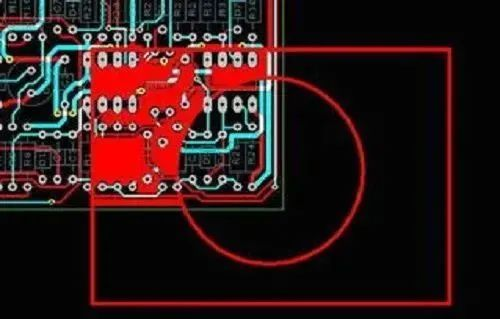
1. Solid Copper Pour
Advantages: Provides both increased current capacity and shielding.
Disadvantages: During wave soldering, the board may warp or even blister.
Solution: Typically, slots are cut into the solid copper to relieve stress and reduce blistering.
2. Grid Copper Pour
Advantages: From a thermal perspective, the grid is beneficial (it reduces the heated copper area) while still providing some electromagnetic shielding.
Disadvantages: A pure grid copper pour is mainly for shielding; its current‑carrying capacity is reduced.
Pros and Cons of Copper Pouring
Advantages:
-
Provides additional shielding protection and noise suppression for inner‑layer signals.
-
Improves PCB heat dissipation.
-
Reduces the amount of etchant consumed during PCB production.
-
Prevents PCB warping during reflow soldering caused by uneven copper distribution and resulting stress differences.
Disadvantages:
-
Copper pours on the outer layers are often fragmented by surface components and signal traces. If there is a poorly grounded copper area (especially long, thin copper slivers), it can act as an antenna and generate EMI problems.
-
If component pads are fully connected to the copper pour, excessive heat sinking may occur, making desoldering and rework difficult.
-
Copper pours on outer layers must be well grounded – this requires adding many vias to connect to the main ground plane, which can reduce routing channels (unless blind or buried vias are used).
Important Considerations for Copper Pouring
To achieve the desired results from copper pouring, the following points should be noted:
-
If the PCB has multiple grounds – such as SGND, AGND, GND, etc. – you should pour copper independently for each, using the dominant "ground" as the reference for its respective area. It goes without saying that digital and analogue grounds should be poured separately. Before copper pouring, first widen the power traces (5.0 V, 3.3 V, etc.) accordingly. This will create multiple differently shaped polygonal structures.
-
For single‑point connections between different grounds, use a 0 Ω resistor, a ferrite bead, or an inductor.
-
For copper pouring near a crystal oscillator – which is a high‑frequency emission source – pour copper around the oscillator and ground its case separately.
-
For isolated islands (dead areas), if they are large, you can add ground vias – it does not take much effort.
-
When starting routing, treat ground traces equally; routes for ground should be laid out properly from the beginning. Do not rely on adding vias after copper pouring to connect ground pins that were left unconnected – that approach does not work well.
-
Avoid sharp corners on the board.
-
Do not pour copper in the empty routing areas of inner layers on multilayer boards – it is very difficult to achieve a "good ground" for that copper.
-
Metal parts inside the equipment – such as heatsinks and metal stiffeners – must be properly grounded.
Summary: If the grounding of copper pours on the PCB is handled properly, the benefits will outweigh the drawbacks – it reduces the return‑path area for signal traces and reduces electromagnetic interference from the board.
That is all about PCB copper pouring – we hope this helps everyone.
About Maxipcb
Maxipcb empowers innovators to turn cutting-edge technologies into reality.We offer one-stop solutions for design, simulation, testing, PCB manufacturing, component procurement and SMT assembly, enabling efficient development, rapid deployment and risk control across the full product lifecycle.
Serving the world in communications, industrial automation, aerospace, automotive, semiconductor and beyond, we build a safer, more connected future together.

