Ground bounce is a type of noise that occurs in transistor switching devices when the PCB ground and the die package ground are at different voltages. To better understand ground bounce, consider the push‑pull circuit below, which produces logic low or logic high outputs.
1. What is Ground Bounce?
Ground bounce is a type of noise that occurs in transistor switching devices when the PCB ground and the die package ground are at different voltages.
To better understand ground bounce, consider the
push‑pull circuit below, which produces logic low or logic high outputs.
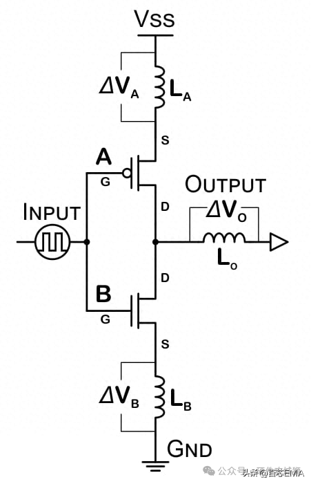
Push‑pull circuit diagram
This circuit consists of two MOSFETs:
- The upper P‑channel MOSFET has its source connected to VDD and drain to the output pin.
- The lower N‑channel MOSFET has its drain connected to the output pin and source connected to GND.
These two MOSFETs respond oppositely to gate voltage:
- A logic low input turns on the P‑channel MOSFET (connecting VDD to output) and turns off the N‑channel MOSFET (disconnecting output from GND).
- A logic high input turns off the P‑channel MOSFET and turns on the N‑channel MOSFET (connecting output to GND).
The tiny bond wires connecting die pads to package pins have small inductance, modeled in the simplified circuit. Stray resistance and capacitance exist but are not modeled for basic understanding.
Equivalent circuit of push‑pull full‑bridge switching with three inductors representing package inductance
After the input has been stable for a long time, the upper transistor connects the output to VDD. Steady magnetic fields form in LO and LA, with zero voltage difference across ΔVO, ΔVA, ΔVB.
When the input switches low, the upper MOSFET disconnects VDD from the output, and the lower MOSFET connects the output to GND. This state change propagates through the system.
2. Causes of Ground Bounce
A voltage difference develops between the output and ground, causing current to flow from the output through the lower MOSFET to ground.
The inductance uses stored magnetic energy to create a voltage difference between ΔVO and ΔVB,
opposing the change in magnetic field.
Even though electrically connected, the voltage between output and ground does not immediately drop to 0 V.
As the output line discharges, the previous voltage difference drives current flow.
Voltage difference induced by package inductance between ΔVB and ΔVO during switching
Inductors LB and LO alter the source and drain voltages of the MOSFETs. This is problematic because the gate voltage is referenced to the die ground.
When the circuit hovers near the gate threshold, the input voltage may fail to hold the gate on or cause
multiple switching events.
When the circuit switches again, a similar mechanism creates a voltage across ΔVA, pulling the source voltage of MOSFET A below the threshold.
3. Why Ground Bounce Is Harmful
When the input changes state, the output and MOSFETs enter an undefined intermediate region, causing
false switching or double‑switching.
All circuits sharing the same GND and VDD connections on the IC are affected.
Ground bounce also disturbs the system ground reference, forcing the PCB GND potential below 0 V.
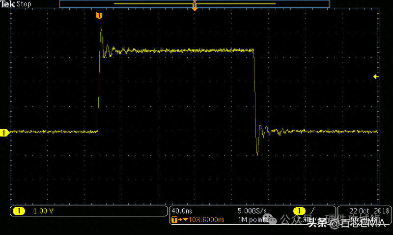
Ground bounce waveform showing ~1 V noise on a 3.3 V rail during switching
When multiple gates switch simultaneously, the effect intensifies and can fully disrupt the circuit.
Noise is not confined to the switching gates: it propagates through shared power and ground rails to other parts of the circuit.
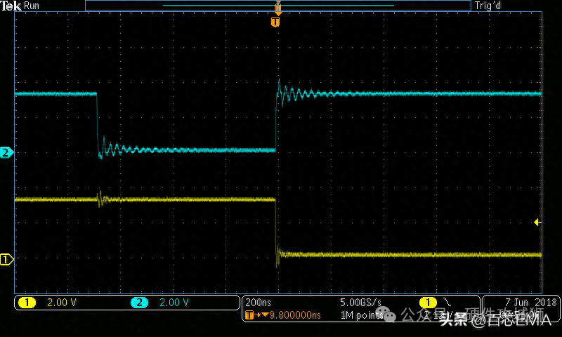
Channel 2 (cyan) shows undamped signal with severe ground/VDD bounce; noise couples to Channel 1 (yellow) signal
4. Methods to Reduce Ground Bounce
1. Use Decoupling Capacitors to Suppress Ground Bounce
The primary solution is to place
SMD decoupling capacitors between each power rail and ground,
as close to the IC as possible.
Distant capacitors add trace inductance and provide little benefit.
When transistors switch, decoupling capacitors supply a
temporary, low‑impedance, stable voltage, limiting bounce and preventing noise from spreading.
Placing capacitors near the IC minimizes the loop area and reduces parasitic inductance.
For mixed‑signal ICs, place decoupling caps on
separate analog and digital power pins.
Connect capacitors to the power plane using
multiple vias.
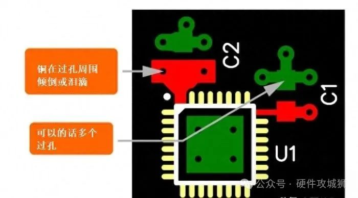
Decoupling capacitor connected to power plane with vias
Use copper pours or teardrops to strengthen via‑to‑trace connections.
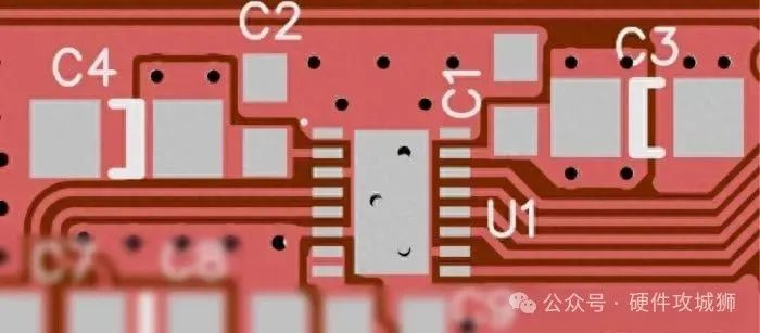
IC (U1) and four capacitors (C1–C4) with copper pad connections
- C1, C2: High‑frequency decoupling capacitors
- C3, C4: Added per datasheet recommendations
If placement near the IC is impossible:
- Mount capacitors on the opposite side of the board directly under the IC.
- Use embedded planar capacitors (parallel copper pours separated by thin dielectric) for very low inductance.
2. Use Current‑Limiting Resistors
Series current‑limiting resistors reduce peak current into and out of the IC.
This lowers power dissipation, prevents overheating, and limits current through MOSFETs,
directly reducing ground bounce.
3. Routing to Reduce Inductance
Keep signal return paths
adjacent to signal traces or on adjacent layers.
Unnecessary separation between signal and return paths increases inductance and ground bounce.
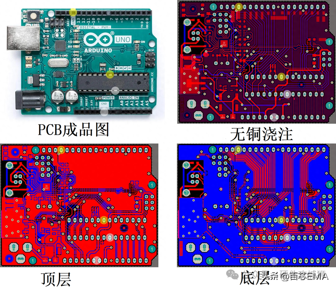
PCB layout with analog ground (white) and digital ground (yellow) highlighted
Separate analog and digital ground returns require careful routing to avoid long, indirect return paths that increase inductance.
4. Reduce Ground Bounce via Programming and Design
Ground bounce worsens with more simultaneous switching outputs (SSO).
Stagger gate switching with small delays to distribute the load.
Example:
- LEDs flashing synchronously create strong bounce.
- Adding a 1 ms offset (imperceptible to users) can reduce bounce by ~3×.
5. Additional PCB Layout Guidelines
- Use via‑in‑pad where design rules allow.
- Minimize signal return path length; place components directly above their ground points.
- Avoid sockets and breadboards.
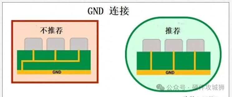
- Do not share ground vias or traces; use dedicated vias and traces to the ground plane.
- Do not connect capacitors directly to outputs.
- Implement LVDS for high bandwidth and noise immunity.
- Choose short‑lead packages (e.g., BGA) to reduce series inductance.
- Use solid ground planes to reduce IR drop and inductance; avoid split ground planes.
- Use lower‑slew‑rate components when possible.
About Maxipcb
Maxipcb empowers innovators to turn cutting-edge technologies into reality.
We offer one-stop solutions for design, simulation, testing, PCB manufacturing, component procurement and SMT assembly, enabling efficient development, rapid deployment and risk control across the full product lifecycle.Serving the world in communications, industrial automation, aerospace, automotive, semiconductor and beyond, we build a safer, more connected future together.