Ball grid array (BGA) packaging has become one of the most popular technologies for integrated circuits requiring high input/output count. BGA packaging has advantages over other methods because of its high-density interconnection ability.
Ball grid array (BGA) packaging has become one of the most popular technologies for integrated circuits requiring high input/output count. BGA packaging has advantages over other methods because of its high-density interconnection ability. With the increasing complexity of integrated circuits and the increasing number of pins and gates, BGA has become the best packaging solution to balance cost and performance. In this guide, we will explain BGA soldering-the process of connecting BGA package to printed circuit board. We will introduce the working principle, solder joint inspection and rework procedure of BGA welding. By understanding ball grid array welding technology, its challenges and solutions, manufacturers can effectively use this advanced packaging technology.
 What is BGA?
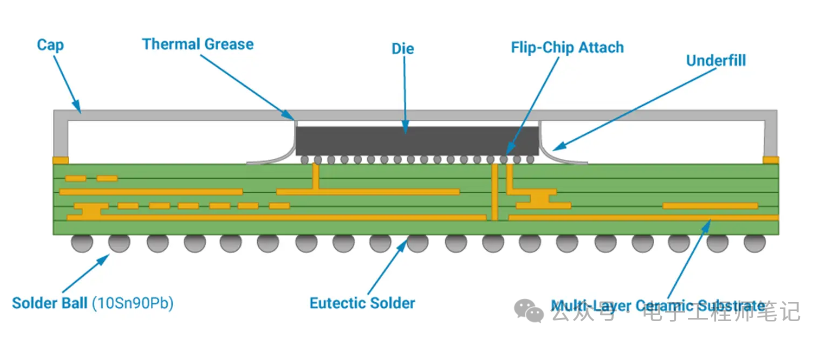
BGA is a unique surface mount package, which is used to fix and install SMD electronic components on the surface of SMT printed circuit board. BGA has spherical leads, which are distributed at the bottom of the package in an array. The ball array is actually named because it is a metal or alloy ball array arranged in a grid.
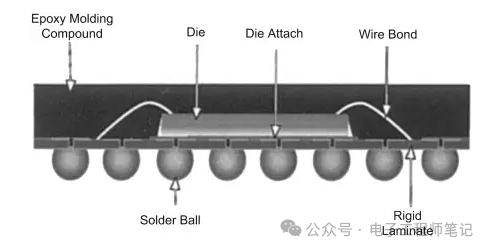
BGA package is used to permanently install devices. It can provide more interconnect pins in which you can place flat or dual in-line packages. The pins used in this technology are solder balls, which are arranged on the lower surface of the package in a certain pattern (usually a grid pattern). This is done to increase the connection area, not just the periphery. The most interesting thing is that through BGA welding, you can benefit from using the whole bottom surface of the equipment, not just the periphery.
This technology is used in various electronic products to install different integrated circuits, such as FPGA, WiFi chip and FPGA. More importantly, these packages are also used in RAM devices, PC chipsets and microcontrollers.
 How BGA soldering works
First, the solder paste is coated on the PCB pad that the BGA solder ball will contact. Solder paste is usually distributed by stencil or screen printing process to ensure accurate and repeatable application.
Then, BGA components are accurately positioned and temporarily fixed on the PCB. This is accomplished by using pick-and-place equipment with high-precision XY motion control and optical alignment system. Correct alignment is crucial.
Then, PCB A is sent to a reflow oven with a specified temperature curve. The solder paste melts, and the solder balls of BGA melt and fuse with the PCB pads to form solder joints. The profile must be hot enough to reflow the solder without damaging the components.
Finally, after cooling, check whether the solder joint is formed correctly and has no defects. Any required rework is completed by using special BGA rework equipment and procedures.
 BGA solder joint inspection
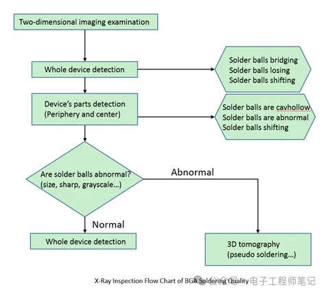
When BGA package was first introduced, there was uncertainty about how to verify solder joints, because they were invisible under the components. Traditional optical inspection methods cannot be used. In addition, electrical tests lack reliability because they only reflect the conductivity of BGA at a specific test time. This method can not predict the long-term durability of solder, and may lead to solder joint failure over time.
In order to really inspect BGA solder joints, X-ray imaging technology is needed. X-rays can penetrate the assembly and capture images of hidden joints. Therefore, when BGA is used to assemble circuit boards, X-ray inspection is very important for process control and quality assurance. X-ray inspection can verify that all joints are completely formed correctly, thus providing the required confidence. Through X-ray, manufacturers can verify their BGA process and ensure the long-term reliability required by these hidden interconnects.
 BGA rework
When the BGA component is found to be defective, it needs to be reworked to remove and replace it. Solder joints must be carefully melted so as not to interfere with adjacent components. This is achieved by BGA rework station, which uses target heat and airflow.
The infrared preheater gently heats the circuit board from below to minimize thermal shock. Thermocouple monitors temperature in real time. After reflow soldering, the vacuum tool will lift the BGA package. Strict process control is essential for success:
Matching solder alloys to ensure joint compatibility
Balance adhesive strength for positioning adjustment.
Strictly follow the prescribed thermal curve.
Use the required minimum airflow setting.
Slowly raise BGA after reflow soldering to avoid scrubbing.
Select the nozzle size that matches the assembly.
With experience and strict procedures, rework BGA can become reliable. But it needs to be very precise and careful to avoid collateral damage. Carefully adjusted processes, professional tools and operator skills are the key drivers of high-quality BGA rework results.
The last thoughtImplementing a robust BGA welding, inspection and rework process requires investment in professional technology, equipment and operator training. But the advantages of higher density BGA packaging make this effort worthwhile in terms of quality and performance. With the expertise in precision printing, accurate mounting, special-shaped reflow soldering, X-ray inspection and controlled rework,
MaxiPCB enables customers to make full use of BGA in key applications. As a leading PCB assembly supplier with nearly 20 years' experience,
MaxiPCB focuses on advanced ball grid array welding technology. Please contact us immediately to discuss your specific BGA project and assembly requirements.


